Hi,
I have several questions on the power and clock of MSP430F5232.
- I could not find a reference design with MSP430F5232. Is there a reference design? I want to check how clocks and powers are provided in the reference design.
- Power: For MSP430F5232, all three powers VCC/AVcc/DVcc are tied together with two capacitors of 10uF and 0.1uF according to the reference design in the user manual (p.21/153 of SLAU278p). Is it a recommended power circuit design?
- Power: I want to estimate the maximum power of the MSP430F5232. According to the table on page 46/104 of "SLAS897-Sept 2013", power can be estimated depending on its frequency when the Vcc is 3.0V. By the way, I am planning to use 3.3V of Vcc. In that case, is there a way of estimating its maximum power? Or is the power going to be very similar to the values shown in the table?
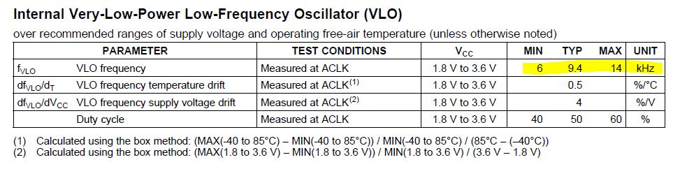
- Clock: Is it necessary to place an external crystal to provide a clock? Or can I use only internal VLO to make uC work?
- Clock:The manual says that XT1 is up to 32kHz while XT2 is up to 32MHz. Is it necessary to provide both XT1 & XT2?
- Clock: If it is required, what frequency is to be used for XT1 & XT2? In other words, what value can be selected? Can I randomly choose any value as long as the value is less than the maximum (XT1 (up to 32kHz) & XT2 (up to 32MHz))?
Thank you in advance.