This thread has been locked.

If you have a related question, please click the "Ask a related question" button in the top right corner. The newly created question will be automatically linked to this question.

MSP430G2432 PWM Output

Other Parts Discussed in Thread: MSP430G2432

Hi Team –

Posting this on customer’s behalf.

We’re looking to generate a PWM output on pin19 of the MSP430G2432, but haven’t had any luck.

We are able to get another CCR register to give the PWM output on pin 6, but nothing on 19. Can you please take a look at the following code, and let us know if something doesn’t look right?


Thank you!


void tmra_init(void)

{

   TA0CTL = TASSEL_2 | ID_3 | MC_1; // SMCLK, 1 MHz, Up Mode

   TACCR0 = 100 - 1;              // 100 us overflow -> 10 kHz Frequency

   TACCTL0 = CCIE;                // Enable Interrupt (Used for 100 us overflow)


   // PWM1 Setup

   TA0CCTL1 = OUTMOD_6;           // Port 2.6 (pin 19) -> PWM toggle/set mode

   TACCR1 = 50;                   // Start at 50% duty cycle

   P2SEL |= BIT6;                 // Port 2.6 (pin 19) -> CCR1 Output


   // PWM2 Setup

   TA0CCTL2 = OUTMOD_6;           // Port 1.4 (pin 6) -> PWM toggle/set mode

   TACCR2 = 30;                   // Start at 30% duty cycle

   P1SEL |= BIT4;                 // Port 1.4 (pin 6) -> CCR2 Output

   P1SEL2 |= BIT4;

}


  • Hello Dan,

    Please make sure when posting code that you use the Rich Formatting editor (link at bottom write of post) and click the </> button to paste in code. This allows the forum to format code for readability. I will modify your post below to follow this.

    As for your question, please make sure the GPIO registers are set appropriately for the pin function you want. This information can be found in the Pin Schematics section of the data sheet. I would explicitly write the P2DIR/P2SEL/P2SEL2 registers to the corresponding value. These registers maybe set to other values else where in the code. In this particular case, the following must be true for timer output for P2.6

    P2DIR.6  = 1

    P2SEL.6 = 1

    P2SEL2.6 = 0

  • Hi Jace,

    I am the customer that is having trouble with this.  Per your suggestion, I added the following lines of code to ensure that those bits were not getting changed in the code.  Unfortunately, it did not fix the problem.  Do you have any other suggestions to try out?

    void tmra_init(void)
    {
    	TA0CTL = TASSEL_2 | ID_3 | MC_1;  // SMCLK, 1 MHz, Up Mode
    	TACCR0 = 100 - 1;			// 100 us overflow -> 10 kHz Frequency
    	TACCTL0 = CCIE;				// Enable Interrupt (Used for 100 us overflow)
    
    	// PWM1 Setup
    	TA0CCTL1 = OUTMOD_6;		// Port 2.6 (pin 19) -> PWM toggle/set mode
    	TACCR1 = 50;				// Start at 50% duty cycle
    	P2SEL |= BIT6;				// Port 2.6 (pin 19) -> CCR1 Output
    
    	// PWM2 Setup
    	TA0CCTL2 = OUTMOD_6;		// Port 1.4 (pin 6) -> PWM toggle/set mode
    	TACCR2 = 0;					// Start at 0% duty cycle
    	P1SEL |= BIT4;				// Port 1.4 (pin 6) -> CCR2 Output
    	P1SEL2 |= BIT4;
    
    	P2DIR |= BIT6;
    	P2SEL |= BIT6;
    	P2SEL2 &= ~BIT6;
    	TACCR1 = 50;	// testing - set to 50% duty cycle
    }
  • Hello John,

    One change I would do is to not set the Timer into up mode until after your other settings are changed. This needs to be the last thing you do for the Timer starts counting as soon as that is set. You may also have to set Bit 7 on this device to the same bit settings found in the Pin Schematics section of the datasheet. P2.6 and P2.7 are linked here for they have to be used in tandem when using a LFXTAL.

    Beyond that, I would place a debug point in your main loop and double check the register settings to make sure everything is setup correctly. It could be something else you are setting up in your code is changing your pin setup.
  • Hi Jace,

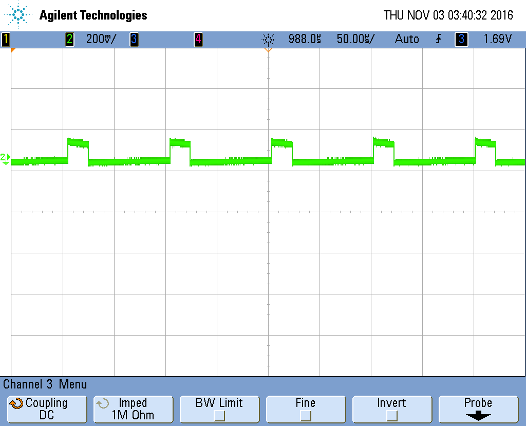
    It seems that we are getting somewhere now.  Once I made those two changes (setting up mode last and setting up Port 2.7), I am now getting an output.  However, it is only going up to ~100 mV (see the attached scope image).  

    void tmra_init(void)
    {
    	//TA0CTL = TASSEL_2 | ID_3 | MC_1;  // SMCLK, 1 MHz, Up Mode
    	TACCR0 = 100 - 1;			// 100 us overflow -> 10 kHz Frequency
    	TACCTL0 = CCIE;				// Enable Interrupt (Used for 100 us overflow)
    
    	// PWM1 Setup
    	TA0CCTL1 = OUTMOD_6;		// Port 2.6 (pin 19) -> PWM toggle/set mode
    	TACCR1 = 50;				// Start at 50% duty cycle
    	P2SEL |= BIT6;				// Port 2.6 (pin 19) -> CCR1 Output
    
    	// PWM2 Setup
    	TA0CCTL2 = OUTMOD_6;		// Port 1.4 (pin 6) -> PWM toggle/set mode
    	TACCR2 = 30;				// Start at 0% duty cycle
    	P1SEL |= BIT4;				// Port 1.4 (pin 6) -> CCR2 Output
    	P1SEL2 |= BIT4;
    
    	P2DIR |= BIT6;
    	P2SEL |= BIT6;
    	P2SEL2 &= ~BIT6;
    
    	// Port 2.7 Setup
    	P2SEL &= ~BIT7;
    	P2SEL2 &= ~BIT7;
    
    	TACCR1 = 20;	// testing - set to 50% duty cycle
    
    	TA0CTL = TASSEL_2 | ID_3 | MC_1;  // SMCLK, 1 MHz, Up Mode
    }

  • Hi Jace,

    You can disregard this message. I changed scope probes and I'm getting the correct level output. Seems the probe or scope channel isn't working correctly. Thanks for helping me fix it!

    Take care,
    John

**Attention** This is a public forum