Other Parts Discussed in Thread: CC1150,
Hi to all,
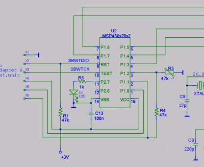
Had to add temperature reading to an earlier project by reading a voltage from half bridge formed by fixed resistor and NTC. It is battery powered device so I wanted to use P1.1 as output to supply power to R/NTC circuit during the a/d conversion only. The output will go to Vcc (cca 3.1V Li battery) if not loaded, but even slightest loading (~100k -> 47K+NTC47K) produces drop like on the picture below:

A trace is output on P1.1 pin and B trace is Vcc.
DS values for Vout gives practically Vcc for such a light loading (Vcc-0.25V @ -1.5mA).
To be sure that some part of firmware is not messing up pin configuration I moved pin setup jut before R/NTC reading:
WDTCTL = WDTPW + WDTHOLD;
P1OUT &= ~BIT1;
P1SEL &= ~BIT1;
P1DIR |= BIT1;
ADC10AE0 = 0x00;
P1OUT |= BIT1;
TI_CC_Wait (1000); // 1000uS wait to allow Uin to stabilize, a/d would go after this
P1OUT &= ~BIT1;
Any hint/direction would be appreciated
Best
Hrvoje