This thread has been locked.

If you have a related question, please click the "Ask a related question" button in the top right corner. The newly created question will be automatically linked to this question.

MSP430FR58471: JTAG Mode Power Draw

Part Number: MSP430FR58471
Other Parts Discussed in Thread: MSP430F2252

Hi,

My customer has the following concern, could you please recommend a solution?

We are using an MSP430FR58471 as a system controller on our latest
family of boards (where previously we have used the MSP430F2252).
Something new we are running into is a high power draw state that
occurs when the part is put into JTAG mode. We do not have this issue
with the MSP430F2252. We are hoping there is some port config we are
not familiar with on this part that needs to be setup after the part
gets put into JTAG mode. Is there anything you can tell us or point us
to?

Thanks,

Chuchen

  • Hi Chuchen,

    Could you provide more details about your customer's issue? Do they have the same issue with code examples?

    Regards,
    Ling
  • Hi, 

    I'm the actual engineer currently working with the MSP430FR58471 and this issue in particular so hopefully I can give a little more context.

    Our mcu has a somewhat complex set of P1-4 port pin connections that make it difficult to measure our target power draw using the sample code. If it comes to that I'll put the time in to appropriately config those pins in one of the examples but even then you'll need snippets of our schematics and connected part pin descriptions as well. Before going down that path I'd like to say that I'm fairly confident that the pin configs I'm setting are correct, or at least not the source of this particular issue.

    I've seen what having a misconfigured pin looks like in terms of power draw and this issue behaves differently. My hypothesis is that there is something that is not being cleared by a chip reset (asserting/releasing reset pin) and is related to the JTAG module. This bad power state only occurs when we do not completely disconnect all power from the mcu after sending the JTAG sequence to the PJ pins. I believe that this is causing the JTAG module to stay on even after a chip reset.

    I've looked through the user guide, data sheet, and errata for this mcu and have yet to see a register with an enable bit for the JTAG module. I would really like to know what register operations will ensure the JTAG module is inactive like in the case of a low voltage BOR reset. I've taken a look at the SYSCTL, SYSJMBC, and PMMCTL among others but haven't found what I was looking for. Will the software locking feature of the JTAG password registers put the JTAG module in a disabled state?

  • I've gone ahead and confirmed that this high power draw state occurs using the msp430fr59xx_lpm3_02.c example code from slac536j.zip. I've only edited it to remove the WDT isr.

    #include <msp430.h>
    
    int main(void)
    {
      WDTCTL = WDTPW | WDTTMSEL | WDTSSEL_2 | WDTIS_5; // VLOCLK, 1s interrupts
      // SFRIE1 |= WDTIE;                          // Enable WDT interrupt
    
      // Configure GPIO
      P1OUT = 0;
      P1DIR = 0xFF;
    
      P2OUT = 0;
      P2DIR = 0xFF;
    
      P3OUT = 0;
      P3DIR = 0xFF;
    
      P4OUT = 0;
      P4DIR = 0xFF;
    
      PJOUT = 0;
      PJDIR = 0xFFFF;
    
      // Disable the GPIO power-on default high-impedance mode to activate
      // previously configured port settings
      PM5CTL0 &= ~LOCKLPM5;
    
      // Clock System Setup
      CSCTL0_H = CSKEY >> 8;                    // Unlock CS registers
      CSCTL1 = DCOFSEL_0;                       // Set DCO to 1 MHz
      CSCTL2 = SELM__DCOCLK | SELS__DCOCLK | SELA__VLOCLK;
      CSCTL3 = DIVA__1 | DIVS__1 | DIVM__1;     // Set all dividers to 1
      CSCTL4 = LFXTOFF;
      CSCTL0_H = 0;                             // Lock CS registers
    
      // P1DIR |= BIT0;                            // Turn on LED
    
      __bis_SR_register(LPM3_bits | GIE);
      __no_operation();                         // For debugger
    }

    Nominal current draw occurs after I program the part via JTAG and then disconnect and reconnect the 3V battery. The current measured is ~0.6uA.

    The high current draw occurs after I program the part via JTAG (or even simply pass the JTAG sequence) and never disconnect power. The current measured is ~129uA.

  • Hi Robort,

    Thanks for the inquiry. I am researching this and will provide you with an answer tomorrow.
    By the way, is this a real user case? Usually the device should be reset after programmed.

    Regards,
    Ling
  • Hi Ling, I appreciate the effort.

    During initial program the device is loaded with an internal 3V battery that has the sole purpose of keeping the MSP alive. Therefore in order to work around this we would need to require users to disassemble the enclosure and disconnect/reconnect the battery every single firmware update for the MSP. Obviously this would be extremely difficult for devices in the field. That being said we do have the RST pin configured for reset function and use that to effect a POR level reset. Unfortunately this does not switch us back to the nominal power draw state. 

  • Hi Robort,

    Did you disconnect the debugger when you measure the current?
    I did some test on FR5969 Launchpad with your code. The current is 130uA when connect the debugger and free run in CCS. And the current is 0.7uA after disconnect the debugger or hardware reset(Reset pin).

    Regards,
    Ling
  • We are not using a TI debugger. We use custom software that handles programming all of our JTAG/flash devices. Support was added to this software to input the JTAG sequence on the JTAG pins to enable the JTAG module and accept standard debug operations. It sounds like this is the problem we are facing, although we need specifics on what happens when the debugger is "disconnected".

    Does a register operation occur on the mcu? Does a JTAG operation need to happen? Does the JTAG pins themselves need some sort of special sequence?

    We have definitely performed a hardware reset (using the RESET pin configured for RESET mode) to no avail.
  • Hi Robert,

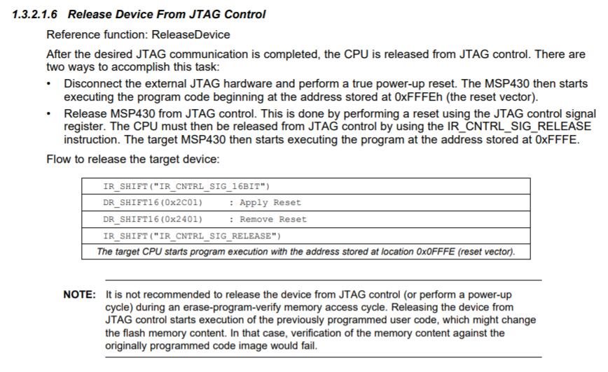
    Have you checked this document?


    Regards,

    Ling

  • I'll forward this to someone who can verify whether or not this is being done. Hopefully I can get back to you with an answer during our regular work hours (~6 hours from now). Thank you for the quick responses!
  • Hi Ling, we're still in the process of attempting to modify our jtag software. In the meantime I would just like to ask once more as clear as I can:

    Is there no possible way to release JTAG control or "disconnect the debugger" from within the mcu itself?
  • No, target device can't be released by master control by itself. It can setup port J if it is in free running mode.
    This device can work just fine with SBW, with only TEST / RESET pin used, without port J.
  • Hi Robert,

    One more question. How do you measure the current? Is it possible that the extra power is from other part of the board?

    Regards,
    Ling
  • We are measuring the current draw via our power supply that is injecting 3V across the battery connector for the MSP430. Our nominal current draw is 1uA in LPM3 mode which goes down to 0.6uA when using the sample code provided previously. When put into this JTAG mode where we see ~130uA, there is no current fluctuation when interacting with any of the board pins (e.g. pulling all pins besides RST/VCC/GND high or low), so I don't believe this is anything external.

  • Hi Robert,

    sorry for the delay on this topic. To answer your question on the possibility to reset JTAG from the CPU side, the most powerful action you can perform is to generate a SW BOR. The respective bit for this is placed in the PMMCTL0 register. It's the PMMSWBOR.

    If this does not resolve the problem, then most probably, there is no other solution, than using the JTAG communication. The reason is basically the system philosophy behind the JTAG/Debug logic - CPU relation. The JTAG needs to be able to control the CPU side of the device not vice versa, as this would generate other non solvable problems.

    Best regards

    Peter

  • Apologies for the late response. We've identified and fixed the issue. After looking closer at the aforementioned document www.ti.com/.../slau320ac.pdf and figure 1-12 specifically, we realized that we were erroneously enabling the BSL entry. After applying the appropriate entry sequence, we did not see our large current draw.

    On a side note, using the software BOR via the PMMCTL register had no effect.

    Thanks to everyone for the help.

**Attention** This is a public forum