This thread has been locked.

If you have a related question, please click the "Ask a related question" button in the top right corner. The newly created question will be automatically linked to this question.

MSP430FR5972: DRV10983: Different addresses for the same slave?!

Part Number: MSP430FR5972
Other Parts Discussed in Thread: DRV10983, TIDA-01373

Good Morning everybody!

Today I'm here because I noticed two different information in two related user guide for the same device and I really don't know what is the exact one.

Let me explain better what I mean.

I need my processor MSP430FR5972 to control a brushless motor and I want them to communicate via I2C. I use DRV10983 motor driver, so I downloaded and started to study

  • SLVUB30A --> User's Guide for the TIDA-01373 Quick Start Guide
  • DRV10983 12- to 24-V, Three-Phase, Sensorless BLDC Motor Driver Datasheet

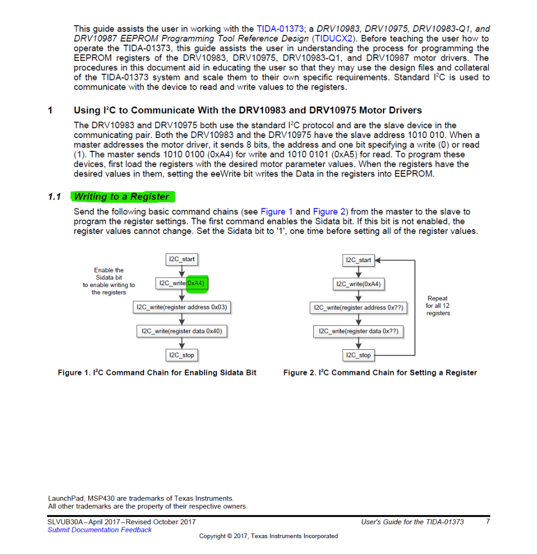
In the first chapter of the Quick Start Guide, the first paragraph is about how to write to a register. Below you have the screenshot of the page I'm talking about.

In chapter 8 at paragraph 5 of the datasheet I read:

Which is the right slave address that I have to write?

Thanks & Kind Regards,

MariaAngela

  • Hello Maria,

    the second document shows 7 bits.
    If you add 0 at the end you would get 0xA4.
    Try with 0xA4 and if that does not work try another address.
    When fixed, please use "Submit Documentation Feedback" link on the pdf footer to tell TI team about this error.
  • "1010 010" and "101 0010" are the same 7 bits. For the MSP430 I2C unit, they are stored right-justified (0x52) in the I2CSA register. The difference between 0xA4 and 0xA5 is the R/W bit, which is not part of the slave address, rather it is appended by the I2C unit based on the UCTR bit.

    Is "I2C_write()" an actual API function, or a piece of code you have to write? If the former, you should go with the (left-justified) convention required. If the latter, you are free to design it using 0xA4/5 (which you shift right 1) or 0x52 or even "(0xA4 >> 1)" to make it obvious.

    Keep in mind that that first I2C_write() is special, since you never explicitly "transmit" the address byte when using the I2C hardware (rather it's done automatically as part of the "Start" operation).

    This left-justified/right-justified documentation thing has been going on for many years; the only thing I know to do is read very carefully.
  • Hi Bruce! Hi Tomasz!

    First of all thank you for your answers and your explanations; they were a really useful starting point for my tests.  

    However I have another question...

    I need my processor to communicate not only with a brushless motor, as I mentioned in the first post, but also with 24LC16 EEPROM and I have some problems with both these slaves in reading mode.

    If I write the I2C_reading function as explained in the programming guide for DRV10983 and also in 24LC16 it seems that I have to send 2 different addresses for writing and reading operation.

    • 0xA4 and 0xA5 for DRV10983 
    • 0xA0 and 0xA1 for 24LC16 

    With this addresses configuration the reading operation doesn't work and gets stuck after the first byte read as 0xFF.

    On the other hand if I write I2C_reading function with the same slave address for writing and reading operations it seems I can get some feedback both from my DRV registers and my EEPROM.

    And, if I understand correctly what you explain me in the previous posts this behaviour depends by setting/clearing UCTR bit. Is it correct?

    If I'm in this scenario, sorry but I really don't understand why providing 2 different addresses for write and read operation if UCTR bit is the key bit for choose between RX/TX mode.

    I'd really appreciate any help to understand better this situation.

    Thanks a lot & Kind Regards,

    MariaAngela  

  • Maria,

    lets assume that in your architecture, MSP430FR5972 would act as a master.

    I2C uses 7 or 10 bits addressing.
    Lets focus on 7 bits.
    7 bit addresses are left justified and LSB (in our case UCTR) determines next operation on a bus.
    UCTR=0, master would act a receiver.
    UCTR=1, master transmitter.
    Both modes are presented on:
    Figure 32-13. I2C Master Receiver Mode
    Figure 32-12. I2C Master Transmitter Mode
    within MSP430FR59xx Family User's Guide.

    <<< I have to send 2 different addresses for writing and reading operation.
    No, you send the same 7bits address and LSB determines reading or writing.

    <<< this behaviour depends by setting/clearing UCTR bit. Is it correct?
    Correct.

    <<< I really don't understand why providing 2 different addresses for write and read operation if UCTR bit is the key bit for choose between RX/TX mode.
    Now we now that RT/TX have the same address.

    <<< if I write I2C_reading function with the same slave address for writing and reading operations it seems I can get some feedback both from my DRV registers and my EEPROM.
    You need to use the same address for reading and writing.

    <<< However I have another question...
    I such a case it is recommended to close the original post and start a new one.
    New topic could help to find better / faster response.
  • Thak you very much for your complete explanation Tomasz!
    Now everything is clear in my mind.

    Kind Regards,
    Maria Angela

**Attention** This is a public forum