This thread has been locked.

If you have a related question, please click the "Ask a related question" button in the top right corner. The newly created question will be automatically linked to this question.

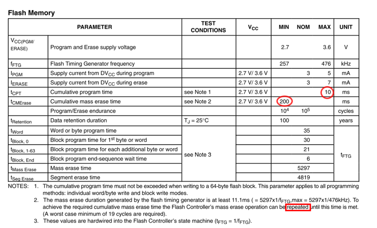
MSP430F449: How to understand "cumulative program time" on Flash program.

Part Number: MSP430F449

Hi TI guys,

I'm now working on a OTA upgrade project use MSP430F449. and confused by the notion:cumulative program time and cumulative .mass erase time. Need your help. :)

If chose the fastest  fFTG= 476KHz ,that means Tftg= 1/476KHz=0.0021ms

Program a byte need 35 fFTG, about 0.0021x35=0.0735ms

If  cumulative program time is 10ms , that makes 10ms/0.0735=136 byte.

Does it mean the input parameter Lenth can't larger than 136?

Besides, how to understand cumulative .mass erase time?  Iam puzzed with NOTES 2 .

B.R

Seafesse

void MSPBoot_MI_WriteBytes(uint16_t Flash_adr, uint08_t* Sram_adr,
                            uint08_t Lenth)
{ 
    uint16_t i;
   // fFTG = 476KHz (Max)
    FCTL2 = FWKEY + FSSEL_2 + FN0 + FN1 + FN2;
    FCTL3 = FWKEY;
    FCTL1 = FWKEY+ WRT;    
    for(i=0;i<Lenth;i++)
    {
        while(0 ==(FCTL3 & WAIT) );
        *( (uint08_t*)Flash_adr ) = *Sram_adr;  
        Flash_adr++;
        Sram_adr++;
    }
    FCTL1 = FWKEY;  
    while( BUSY & FCTL3);
    FCTL3 = FWKEY + LOCK;
}

  • Hi SeaFesse,
    there are two main aspects with the FLASH related operations erase and write to FLASH.

    Lets start with the erase and cumulative erase time. An erased FLASH cell is set to logic one. This means, the respective cell, if previously set to 0, needs to be charged up again. Now the charge process requires the application of a higher voltage, generated by internal circuitry, but still does not happen within an arbitrary short time. It is like charging up a capacitor, to reach a certain level of charge.
    So translating this to the FLASH erase operation means, one has to apply the charge voltage for a certain minimum time, to ensure the cells being charged up properly, to be recognized as 1s and guarantee the life time of the charge, means data retention.

    Now to FLASH writes. For writing to FLASH also higher voltages need to be applied, though basically discharging the cells, which need to be set to 0, and leave the ones which need to stay 1s as they are. Still the application of the higher voltage causes higher leakages of the cells, means the content/charge even of the not discharged cells is degrading. To maintain the specified data retention time and cell information, the stress, means cumulative programming time should not be violated. Cumulative time means in this case write accesses before applying erase, and thus restoring the respective cells. That's why to be able to write a full block of FLASH, without violating the cumulative programming time, one should use word access instead of byte access, as the write of a byte takes the same time as the write of a word, but writing a block word wise takes just half of the cumulative time.

    You can find further details on this in the User's Guide chapter "FLASH Memory Controller".

    Best regards
    Peter
  • Hi Peter,
     Wow~ thanks for your vivid explannation, that helps a lot.

    So only "Block write" has the precondtion of cumulative program time ,am I right?

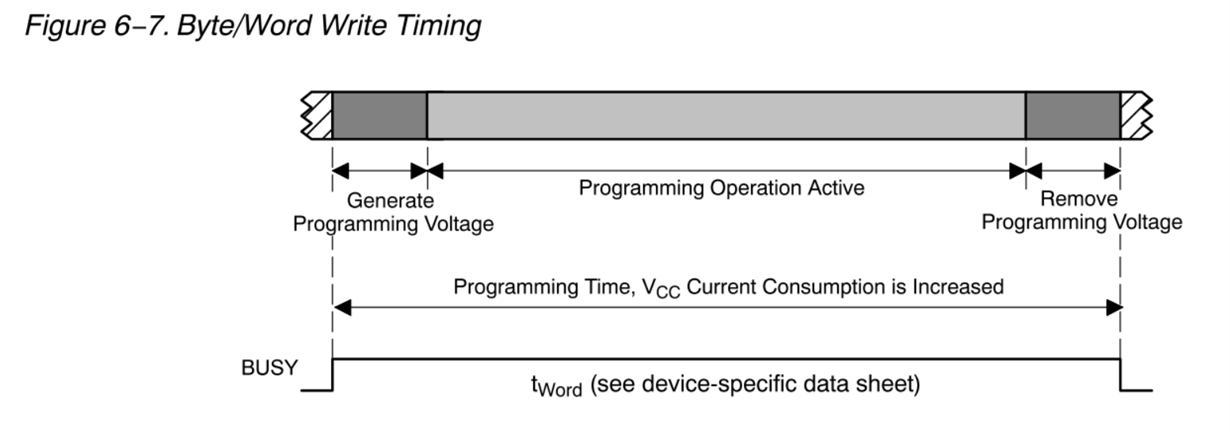
    I find no bytes(words) limiting condition on byte/word program on user guider.

    So the fuction MSPBoot_MI_WriteByte can write as many words as i wish when called once?


    B.R

    SeaFesse

  • Hi SeaFesse,
    you're correct, for byte and word write, there would not be a violation of the datasheet parameters. Still please keep in mind there is a degradation due to the stress caused by the programming voltage. Thus writing as short as possible, is better.

    Best regards
    Peter

**Attention** This is a public forum