This thread has been locked.

If you have a related question, please click the "Ask a related question" button in the top right corner. The newly created question will be automatically linked to this question.

CCS/MSP430F5152: MSP40F51x2 high resolution timer D0 / D1 is not synchronized with TEC clear command (TEC1XCTL2 |= TECAXCLREN)

Part Number: MSP430F5152
Other Parts Discussed in Thread: MSP430WARE

Tool/software: Code Composer Studio

Hello MSP430 expert, 

 I've been designing MPPT controller by referring PMP7605 reference S/W using MSP430F5152 MCU.  

As Timer D0/D1 is documented that it have problem in using up/down mode to make proper dead time in high resolution mode ,

I tried to synchronize timer D1/D1 using TEC clear command TEC1XCTL2 |=TECAXCLREN & TD0CTL0 |= TDCLR;.

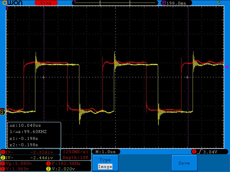
In spite of using the same value to TD0CCTL0/1/2 and TD1CCTL0/1/2, the generated PWM waveform is not synchronized.

But make about 800nsec timing difference gap as the attached scope capture.  The S/W routine is also attached.

Could you pls advise what’s wrong ?

unsigned int Duty =304, Deadtime =25;

{

        Get_TLV_Info(TLV_TIMER_D_CAL, 0, &bTD0CAL_bytes, (unsigned int **) &pTD0CAL);

                                                       //Get TimerD0 Cal Values (instance 0)

        if(bTD0CAL_bytes == 0x0)

        {

           // No TimerD free running cal data found

           while(1);                             // Loop here

        }

        // Configure Master Timer Instance - TimerD0, Hi-Res Calibrated Mode

        TD0CTL0 = MC_1 + TDSSEL_2;                       // TDCLK = SMCLK = 25MHz = Hi-Res input clk select

        TD0CTL1 |= TD2CMB + TDCLKM_1;                     // Select Hi-res local clock

        TD1CTL0 |= MC_1 + TDSSEL_2;    // up-mode,

        TD1CTL1 = TD2CMB + TDCLKM_2; // TD1 clock = Auxiliary clock source from master timer instance


        TD0HCTL1 = pTD0CAL->TDH0CTL1_128;         // Read the 128Mhz TimerD TLV Data

        TD0HCTL0 = TDHEN + TDHM_0;               // CALEN=0 => free running mode; enable Hi-res mode

        TD1HCTL0 = TDHEN + TDHM_0;               // CALEN=0 => free running mode; enable Hi-res mode                                        

        // Here Timer D is configured to run at 128Mhz


        TD0CCR0 = 696;                           // 1ch TimerD run for non-interleaved

        TD0CCR1 = Duty - Deadtime;               // High side PW_H1 >> PW_H2

        TD0CCR2 = 696 - Deadtime;                 // Low Side PW_L1 >> PW_L2

        TD0CCTL2 |= OUTMOD_7;                     // TD1CCR2, Set/reset


        TD1CCR0 = 696;                  // 128M/696 = 182.xxKhz is the operating frequency of the buck stage

        TD1CCR1 = Duty - Deadtime;               //

        TD1CCR2 = 696 - Deadtime;

        TD1CCTL2 |= OUTMOD_7; //+ CLLD_1;                    // TD0CCR2, Set/reset


        // Syncronize master (TD0) and slave (TD1) timer instances

//

        TEC1XCTL2 |= TECAXCLREN;         // Enable synchronized clear by enabling Aux clear of slave timer

//      TEC0XCTL2 = TECAXCLREN;          // Enable synchronized clear by enabling Aux clear of slave timer

        TD0CTL0 |= TDCLR; // + TDCLGRP_1; clear TDR, Start timer -UP

//      TD1CTL0 |= TDCLR; //+ TDCLGRP_1;      TD1CCTL2 = OUTMOD_7 ;//+ CLLD_1;

        TD0CCTL2 = OUTMOD_7 ;// + CLLD_1;   TD1CCTL1 = OUTMOD_7 + CLLD_1;

        Init_IOs ();


}


void Init_IOs (void)

{

   P2SEL |= BIT0 + BIT3; // BIT0 // P2.0/TD0.2, P2.2/TD1.1, P2.3/TD1.2, options select

   P2DIR |= BIT0 + BIT3 + BIT6 + BIT7;   //,

Thanks,

YS Kim  

  • Hi Yongsung,

    As a first step - before digging into the code. Are you able to review section 20.2.5, page 552 of the MSP430x5xx and MSP430x6xx Family User's Guide.

    This section details the synchronization mechanism between the Timer_D instances for this device.

    Let me know if you have had a chance to look at this first - and if it helps with your issue.

    Thanks,

    -Chris

  • Hi Chris, 

     Thanks for the advice ! 

    Even I use the exact same code that user's guide  p552,   still same problem is observed.  

    To verify the timing,   I used the same value 200 on TD0CCR0 and TD1CCR1,  and same 40 to TD0CCR1 and TD1CCR1,  

    and same 80 on TD0CCR2 and TD1CCR2.    Then PWM freq become 854KHz and TD0 - TD2 delay become about 180nsec. 

    measurig point is TD0.2 and TD1.2.   Never be synchronized.     

    And even there is TEC1XCTL2 SFR in MSP430F5152 per datasheet,  CCS do not show TEC1XCTL2 in register watch screen. 

     Only show TEC0X... registers.  .      

    To focus only the timerD timing issue,   I  deleted all the other pherpheral related code ADC, DMA,  WDT, UART and etc.

    Remained only  main () code which include clock init , tmerD init and IO init or test. 

     What would be the problem ?        

    -------------------------------------------- 

    void Init_Timer (void)
    {

     TD0CTL0 = TDSSEL_2;                       // TDCLK = SMCLK = 25MHz = Hi-Res input clk select
     TD0CTL1 |= TDCLKM_1;                      // Select Hi-res local clock
     TD0HCTL0 = TDHEN + TDHREGEN + TDHM_0;

     // TD1HCTL0 = TDHEN + TDHM_0;                // CALEN=0 => free running mode; enable Hi-res mode                                           // TDHM_0 => 128Mhz, TDHM_1 = > 256Mhz
     // Here Timer D is configured to run at 128Mhz
     TD1CTL1 = TDCLKM_2;                       // TD1 clock = Auxiliary clock source from master timer instance

     TEC1XCTL2 |= TECAXCLREN;      // Enable synchronized clear by enabling Aux clear of slave timer

     TD0CTL0 |= TDCLR; // + TDCLGRP_1;

     TD0CCR0 = 200;                            //                              1 ch TimerD run for non-interleaved
     TD0CCR1 = 40;                // High side PW_H1  >> PW_H2
     TD0CCTL1 |= OUTMOD_7;                     // TD1CCR1, Reset/Set
     TD0CCR2 = 80;                  // Low Side PW_L1  >> PW_L2
     TD0CCTL2 |= OUTMOD_7;                     // TD1CCR2, Set/reset

     TD1CCR0 = 200;                            // 128M/700 = 182.8Khz is the operating frequency of the buck stage
     TD1CCR1 = 40;                // High side PW_H1  >> PW_H2
     TD1CCTL1 |= OUTMOD_7; //+ CLLD_1;                     // TD0CCR1, Reset/Set (outmode2-> toggle &reset ?)
     TD1CCR2 = 80;
     TD1CCTL2 |= OUTMOD_7; //+ CLLD_1;                     // TD0CCR2, Set/reset

     TD0CTL0 |= MC_1 + TDCLR; // + TDCLGRP_1;                  // up&down-mode, clear TDR, Start timer -UP&down -Modified by YSK

    }

    YS Kim


  • Yongsung,

    Thanks for the helpful information. Have you tried clearing TD0 after it starts to count?

    Please see the image below of the note on Section 19.3.1, page 554, of the MSP430x5xx and MSP430x6xx Family User's Guide.

  • Hi Chris, 

     I've fixed the TD0/TD1 async problem using Timer D regulation  mode (TDHREGEN = 1) by referring  MSP430ware example.      

    Since it can cause  interrupt by setting TDHLKIE = 1,     I put  'TD0CTL0 |= MC_1 + TDCLR'  on TDHKIFG interrupt vector service routine.  

    And also cleared counter 'TD0CTL0 |= MC_1 + TDCLR'  when TD0CCTL0 interrupt occurred.  And cleared counter again when I change

    TDxCCRx value.  

    But not sure on non-regulation free runing clock mode since it cannot genrate high res freq lock interrupt.   Only when TD0CCTL1 / TD0CCTL2 = CCIE. 

    Thanks for the attention for the issue ! 

    YS Kim


**Attention** This is a public forum