This thread has been locked.

If you have a related question, please click the "Ask a related question" button in the top right corner. The newly created question will be automatically linked to this question.

MSP430F2002: Sporadic abormal CPU behaviour after PON

Part Number: MSP430F2002

Hi champs,

after startup MCU sometimes shows a non expected behaviour (try to get more information from customer).

During this abnormal state, power consumption is significant lower (my not confirmed assumption: CPU clock is much lower than expected).

This behaviour can only be seen without JTAG debugger!

CLK is configured at beginning of code. A workaround seems to insert 2 x __no_operation() to bypass tis behaviour.

Only one __no_operation()  does not work secureley!

Customer thought erratum BCL12 can be applied, but code is executed after PON, so very unlikely.

Here is code sequence:

  /* Set the MCLK to 12MHz calibrated */

  DCOCTL = 0;                /* Select lowest DCOx and MODx settings */

  BCSCTL1 = CALBC1_12MHZ;    /* Set range */

  DCOCTL = CALDCO_12MHZ;     /* Set DCO step + modulation */

  BCSCTL2 |= DIVS_2;         /* SMCLK = 3 MHz */

  __no_operation();

  __no_operation();


Q: Why are 2 x __no_operation() needed and is this a valid workaround  to ensure stable execution in mass production ?


  • Hi,

    could you please give us more details on the customer's setup? We need supply voltage plots.

    It would also be good to insert the generation of a trigger signal on a GPIO, toggling a pin, to be able to monitor the status of the supply voltage at the point where the Clock System manipulations are executed.

    My suspicion is an overclocking of the CPU.

    Another test in that direction would be inserting a wait loop before the clock register manipulations. If this also resolves the issues, would be confirming the overclocking theory.

    We of course also need the information about the used supply voltage as such.

    The insertion of two consecutive nops removes the changes on the data bus system, which reduces the risk of overclocking. Of course also dependent on the following instructions.

    But let's make one step after another.

    Best regards

    Peter

  • Peter,

    customer will be out some days and answer later..stay tuned !

    -Dirk

  • Peter,

    here is answer:

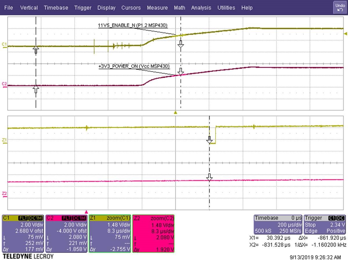
    I have built in a toggle of P1.2 around the CLK configuration. Vcc of MSP430 is then about 1.9V, which is too low for 12MHz. What behavior can be expected when the MSP430 is overclocked?


    As a workaround, there are three options:

    • A wait before the CLK configuration (about 0.5ms) -> it is tested and works
    • A faster start of Vcc
    • An external reset device that only releases the reset signal above Vcc = 2.7V. -> it is tested and works


    Start of the firmware:

      P1DIR = BIT2;       /* testcode P1.2 output, else input */

      P1OUT = BIT2;       /* testcode P1.2 high */

      /* Set the MCLK to 12MHz calibrated */

      DCOCTL = 0;                /* Select lowest DCOx and MODx settings */

      BCSCTL1 = CALBC1_12MHZ;    /* Set range */

      DCOCTL = CALDCO_12MHZ;     /* Set DCO step + modulation */

      BCSCTL2 |= DIVS_2;         /* SMCLK = 3 MHz */

      P1OUT = 0;          /* testcode P1.2 low */

  • Hi,

    this confirms my suspicion. The device is definitely overclocked in this scenario. The possible effects are more or less unpredictable. The CPU can, dependent on the to be executed instructions and data, generate all kind of errors.

    Thus the customer needs to address this by one of the options he listed. Basically you can boil it down to the requirement "The customer needs to ensure, he is clocking the device with a clock frequency (be also mindful of duty cycle of the clock / in this case not really applicable, as DCO is being used, but in case of crystal or ceramic resonators, this could apply...), which is in relation to the used supply voltage within the specified range under all conditions."

    All three mentioned options can work, though a pure timing based solution is the most risky one, as if for what ever reasons the supply voltage should start slower, the device could fail again.

    Just to mention, though potentially not so critical. Also the shut down phase can be a problem, if the customer operates the device during shut down with 12MHz. Especially when any FLASH modifying code should be present in his application. The CPU could jump erroneously into the FLASHing routines and corrupt FLASH content.

    Thus supervising the supply voltage directly, is certainly a better approach.

    Best regards

    Peter

**Attention** This is a public forum