This thread has been locked.

If you have a related question, please click the "Ask a related question" button in the top right corner. The newly created question will be automatically linked to this question.

CCS/MSP430F6638: MSP430F6638 debugger and debug connector

Part Number: MSP430F6638
Other Parts Discussed in Thread: MSP-FET, AFE4403

Tool/software: Code Composer Studio

Hello,

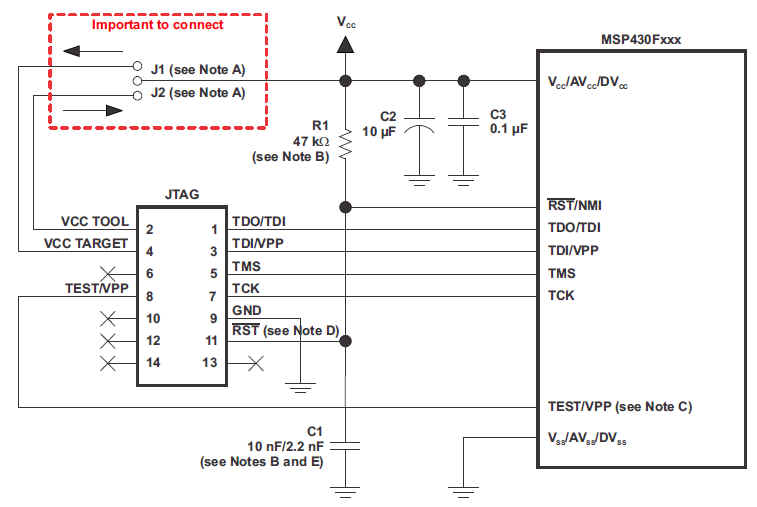
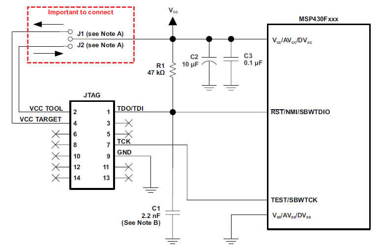
We are actually working on a project and we are going to use the MSP430F6638 MCU. So basically we need a debugger in order to debug the code inside the MSP430F6638. So which debugger do you recommand us to use ? The MSP-FET debugger could be a good solution ? We have taken a look at the MSP debuggers user guide and we found out that we should use a 14-pin JTAG connector with the MSP-FET, right (picture below) ? 

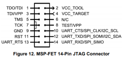
Since the MSP430F6638 doesn't have a RTS pin how should we connect pin 13 with the mcu ? Also for the pin 10,12 and 14, in which situation we have to connect these pins to the UART, SPI or I2C pins of the mcu ? In other words pin 10,12 and 14 should be connected to the uart, spi or i2c pins of the mcu ? And finally since the pin 2 (VCC_TOOL) should be connected to the mcu power supply, where pin 4 should be connected ? It's really important for us to be clear with the debug connector connections since it's often source of error.

Thank you.

Best regards,

Mike

  • Hi Mike,

    First of all, the MSP-FET is the correct one.

    Actually, F6638 supports not only 4-wire JTAG mode, but also 2-wire Spy-Bi-Wire mode for debugging/programming.

    I'm not sure if you missed something, but F6638 should have a RST pin. In the 100-pin PZ package, the RST pin is #96. Please take a second look.

    For 4-wire JTAG interface, you could use this way:

    And for 2-wire SBW interface, you could go with:

    From above two figures you could see that you can leave pin 10/12/14 NC as they are actually not debug related functions. They provide the "BSL" interface.

    Last one, if you want to power up F6638 from the debugger, then you could connect debugger's pin 2 to F6638's VCC; if F6638 is powered up from an external supply, you could either leave pin 2/pin 4 NC or connect pin 4 to VCC as a voltage monitor.

    For the detailed information, you could refer to below doc, and all the figures/info above are also coming from below doc.

    Regards,

    Harry

  • Hello, 

    Thank you very much for your response. In our case we developped a system which uses the MSP430F6638 mcu. The system is powered by a 3.3 V output from a LDO regulator (the input of the LDO is a 3.7 V from a Li-ion battery). This means pin 4 of the JTAG connector should be connected to the 3.3 V power supply, right ? So this is our first question. 

    We have also questions about some other pins of the MSP430F6638 :

    - pin 9 and 10 which are Vref+ and Vref- for ADC and DAC. Since we want in our case a positive reference voltage of +3.3 V for the ADC and DAC and a negative one of 0V, these two pins (9 and 10) should be left NC and then the voltage references have to be set by software or it's absolutely not like that ?

    - pin 16 which is ADC12CLK. We actually use the ADC and DAC channels of the MSP430F6638. Then this pin should be connected or it should be left NC or it shluld be configured by software? Same for pin 34. Should we connect it to a clk source, leave it NC or something else ?

    - pin 88 which is RTCCLK. Actually we are using the RTC but we don't know in which case it could be useful to use this pin ?

    - pin 46 which is SMCLK. As well, in which case this pin could be useful ? We don't know if we have to leave it NC or no. Is this pin used for providing a clock signal to another device who needs a clock ? 

    Thank you very much.

    Best regards,

    Mike Jaber

  • Hi Mike,

    This means pin 4 of the JTAG connector should be connected to the 3.3 V power supply, right ? So this is our first question. 

    Yes, pin 4 of the JTAG could be connected to the 3.3V as a voltage monitor.

    - pin 9 and 10 which are Vref+ and Vref- for ADC and DAC. Since we want in our case a positive reference voltage of +3.3 V for the ADC and DAC and a negative one of 0V, these two pins (9 and 10) should be left NC and then the voltage references have to be set by software or it's absolutely not like that ?

    For this, F6638 provides three voltage references options: AVCC/AVSS (usually 3.3V), on-chip reference(1.5V/2.0V/2.5V configurable), or external reference from VeREF+/VeREF- pins. If you want to use 3.3V/0V, then it's functionally ok to choose from AVCC and leave the VeREF+/VeREF- NC, but please notice that there are much more noise on the AVCC/AVSS which will definitely affect your ADC's accuracy. From this point, I suggest you to at least use the on-chip reference, or for a higher accuracy choose an external reference IC and along with VeREF+/VeREF- pins.

    - pin 16 which is ADC12CLK. We actually use the ADC and DAC channels of the MSP430F6638. Then this pin should be connected or it should be left NC or it shluld be configured by software? Same for pin 34. Should we connect it to a clk source, leave it NC or something else ?

    The ADC12CLK pin is actually an output pin, which outputs the clock signal used by the ADC, to source to other modules (such as on-chip timer, or external IC) for synchronization. If you don't need this, you can just leave it NC. Same as the RTCCLK/SMCLK pins.


    Besides, please pay more attention to all the pins which are left NC/floating. I suggest you to configure all the floating pins to a fixed status (output high/low) to avoid unexpected current consumption in low-power applications.

    Hope this would help.

    Regards,

    Harry

  • Hi Harry,

    Thank you very much for your asnwers, they've resolved our issues, we will take care about the nc and floating pins, because we are indeed trying to implement a low power consumption system. We have however one further question. As we are using the ADC, we want to set a 100 Hz sampling frequency. Is it possible with the F6638 ? We have checked the user manual of the F6638 ("MSP430x6xx Family" p732) with all these clock sources and divider... However we are a little bit lost about how to set a 100Hz sampling frequency and how these registers should be configured... 

    We noticed that there are two registers ADC12SHT0x and ADC12SHT1x, but we are not sure if these are the registers that give the sampling frequency and how to configure it. Furthermore we are using a 4 MHz quartz for the MCU on XT2IN and XT2OUT pins, and a 32 kHz crystal on XIN and XOUT pins of the MCU (picture below). So we guess we should use ACLK as clock source and select XT2 pins as oscillator source for the ADC but then we are lost with all these dividers predividers and how to set the 100 Hz sampling frequency, without forgetting also that in the datasheet they are talking about XT1 as the oscillator source whereas there is no XT1 pin in the connection pins in the scheme below and XT2 is the main source (4 MHz). 

    We don't know if we did some mistakes or if we misunderstand the user manual but we really didn't find a clear way to set the 100 Hz sampling frequency, and if it's even possible. We are using analog input A0 ADC12_A with ADC12CTL0 Register.

    Thank you.

    Regards,

    Mike

  • Hello Harry,

    Once again thank you very much for your asnwers, they've resolved our issues. We have written a post 2 days ago about ADC12 of F6638 mcu but it's not necessary for you to answer it because we will recap our questions here. As mentionned in the last post we want to set a 100 Hz sampling frequency for the ADC12 of the F6638, which means we want to take a sample of the ADC input signal each 10 ms. After reading lot of documents we noticed that it's possible to create a 100 Hz sampling frequency signal with timers. So we have tried to write some code and implement this signal but we are not sure at all if this is correct, since we are new with MSP430 and we are a little bit lost with all these dividers, clock sources... So here is the code we tried to implement with the timer 100 Hz signal and ADC12 configuration :

    TA1CCR0 = 320; // 100hz sampling frequency 
    TA1CCR1 = 295; // DC of 8%
    TA1CCTL1 = OUTMOD_2; // CCR1 toggle/reset
    TA1CTL = TASSEL_1 + TACLR+ MC_1; // ACLK, up mode
    TA1CCTL0|=CCIE; //  ENABLE CCR0 INTERRUPT

    #pragma vector=TIMER1_A0_VECTOR

    __interrupt void TIMER1_CCR0_ISR(void)
    {
    ADC12CTL0 &= ~ADC12ENC; // ADC12 disabled

    REFCTL0 &= ~REFMSTR; // Reset REFMSTR to hand over control to

    ADC12CTL0 =  ADC12REFON + ADC12ON + ADC12REF2_5V; // ADC12SHT0_2 ?? How to configure it ?

    ADC12CTL1 = ADC12SHP + ADC12SSEL_1; // enable sample timer,aclk

    ADC12MCTL0 = ADC12SREF_1 + ADC12INCH_0; // ADC A0

    ADC12IE = ADC12IE0; // ADC_IFG 

    ADC12CTL0 |= ADC12ENC+ADC12SC; //enable and start convertion
    }

    So this is the code we wrote by reading some examples and refering to the datasheet but we are not sure about some points :

    1) Knowing that we use the timer signal as sampling frequency clock for the ADC, we want at each rising edge of the timer signal the ADC to take a sample of the input signal. Thus, is it right to program an interruption for CCR0 as we did above, instead of programming the interrupt for CCR1 ? We have a doubt about this point because in the datasheet it's specified that the output signal of the timer toggle when the counter reachs CCR1 (picture below). We are using output mode 2. So by programming interrupt for CCR0 instead CCR1 the adc will take a sample at each falling edge and not rising edge, no ? 

    2) In the code above we have enabled interrupt in CCR0 with "TA1CCTL0|=CCIE; //  ENABLE CCR0 INTERRUPT". We have by the way noticed that (p 479 user manual) there is a CCIFG bit. Did we miss this bit in cour code or the code as we wrote it is correct ?

    3) The ADC12CTL0 Register (p750) contains ADC12SHT1x and ADC12SHT0x fields. Since we are using the timer 100 Hz signal, do we have to configure these two fields ? We think that they are not necessary to configure them since it's about ADC12CLCK cycles whereas we are using timer as source clock for sampling frequency.

    4) Furthermore we would like in our code to store in a variable the converted value of ADC and to start a new conversion, only when the previous conversion is completed. To do this, is it right as we did above to program ADC12IE = ADC12IE0; In other words by writing ADC12IE = ADC12IE0 is it enough to get an interruption each time a conversion is completed or do we have instead to use the ADC12BUSY field (p752) of the ADC12CTL1 Register ?

    5) We are not sure about selecting in ADC registers the timer signal as sampling frequency source. Is it correct as we did it by setting ADC12SHP field of ADC12CTL1 Register to 1 ? Or maybe we did a mistake and it's the ADC12SHSx field which configure that ? 

    6) Finally as mentionned in the last post we are using a 32 kHz crystal on XIN and XOUT pins of F6638. We want to source another TI device (AFE4403) with a 4 MHz clock. In order to do this is it necessary as we did to connect a 4 MHz crystal on XT2IN and XT2OUT pins of F6638 or it could be done internaly ? (picture below)

    If yes could we use the SMCLK pin (pin 46 of F6638) to source AFE4403 ? Indeed in AFE4403 TI recommands to use one crystal oscillator (picture below).

    We have chosen the MCU clock as master with the SMCLK (?) pin maybe if possible as the 4 MHz clock out source. However the AFE4403 device has XIN and XOUT pins as input clock pins. Then how should we connect the SMCLK pin with these two pins ? Should we connect SMCLK to both pins ? 

    Thank you very much in advance.

    Best regards, 

    Mike

  • Hi Mike,

    Firstly, it's high recommended that please don't make such configuration in your interrupt service routine (ISR). This will close the door to serve other interrupt if have (in MSP430's ISR the GIE is default disabled thus no interrupt can be asserted during an ISR by default) and may cause big trouble in large project. Actually, getting back to your case, you could get your ADC initialized outside the ISR, and only set the ADC12SC & ADC12ENC bit in the ISR to let the ADC sample and conversion.

    Let me temporarily put your questions away, and try to solve your requirement from the top: You need a 100Hz sample rate ADC here, and the 100Hz is generated by timer. Otherwords, a 100Hz signal generated by timer to trigger the ADC's sample and conversion.

    Taking a look at the User's Guide we found that there are 4 sources for the ADC's trigger.01/10/11 are device specific.

    In F6638's datasheet we found that TA0.1, TB0.0 and TB0.1 are source 01, 10, and 11, respectively. Shown as below for TA0.1:

    Then we could go with TA0.1 configuration, as below:

    TA0CCR0 = 320 - 1; // 100hz sampling frequency 
    TA0CCR1 = 295; // this could be any value smaller than 319. the duty cycle is not important
    TA0CCTL1 = OUTMOD_2; // out mode 2/3/6/7 are all ok
    TA0CTL = TASSEL_1 + TACLR+ MC_1; // ACLK, up mode

    After that, we go with ADC's configuration:

    ADC12CTL0 &= ~ADC12ENC; // ADC12 disabled
    REFCTL0 &= ~REFMSTR; // Reset REFMSTR to hand over control to
    ADC12CTL0 =  ADC12REFON + ADC12ON + ADC12REF2_5V + ADC12SHT0_2; // Sample time 16, around 16/4.8MHz = 3.3us
    ADC12CTL1 = ADC12SHP + ADC12SHS_1; // enable sample timer, ADC clock from MODCLK, trigger source 1
    ADC12MCTL0 = ADC12SREF_1 + ADC12INCH_0; // ADC A0
    ADC12IE = ADC12IE0; // ADC_IFG 
    ADC12CTL0 |= ADC12ENC; //enable convertion

    Here are something you need to pay attention:

    1. SHT0 = 2, means sample time is 16 ADC clock. It's recommended to set this at least to 1, 8 clock, from performance aspect. Longer sampling time also works, but could cause more current consumption. This is required by the datasheet and capacitor charging model:

    2. ADC12SHS = 1. As said previously, this chooses the trigger source.

    3. ADC12SSEL = 0. Using internal clock.

    After ADC/TimerA0 configuration done, you could get a 100Hz sample rate ADC, triggered by timer.

    Then, let me get back to your questions.

    Firstly, I would not recommend you to use ACLK as ADC's clock since there is a MIN conversion clock which is 0.45MHz (450kHz). ACLK is smaller than this which could cause performance loss.

    1) Knowing that we use the timer signal as sampling frequency clock for the ADC, we want at each rising edge of the timer signal the ADC to take a sample of the input signal. Thus, is it right to program an interruption for CCR0 as we did above, instead of programming the interrupt for CCR1 ? We have a doubt about this point because in the datasheet it's specified that the output signal of the timer toggle when the counter reachs CCR1 (picture below). We are using output mode 2. So by programming interrupt for CCR0 instead CCR1 the adc will take a sample at each falling edge and not rising edge, no ? 


    As your original setting, both CCR0/CCR1 interrupt could be used. It doesn't matter which edge ADC samples at. Only the frequency matters, right?

    2) In the code above we have enabled interrupt in CCR0 with "TA1CCTL0|=CCIE; //  ENABLE CCR0 INTERRUPT". We have by the way noticed that (p 479 user manual) there is a CCIFG bit. Did we miss this bit in cour code or the code as we wrote it is correct ?


    I may not catch this question. CCIE is used for interrupt enabling, while CCIFG is the interrupt flag. When the timer interrupt comes, you need to clear this flag (CCR0's IFG is auto cleared thus you don't need to worry about that).

    3) The ADC12CTL0 Register (p750) contains ADC12SHT1x and ADC12SHT0x fields. Since we are using the timer 100 Hz signal, do we have to configure these two fields ? We think that they are not necessary to configure them since it's about ADC12CLCK cycles whereas we are using timer as source clock for sampling frequency.


    Actually since you set ADC12SHP bit, you must configure the ADC12SHT bits accordingly. For detailed information you could refer to 28.2.5 "Sample and Conversion Timing" section.

    4) Furthermore we would like in our code to store in a variable the converted value of ADC and to start a new conversion, only when the previous conversion is completed. To do this, is it right as we did above to program ADC12IE = ADC12IE0; In other words by writing ADC12IE = ADC12IE0 is it enough to get an interruption each time a conversion is completed or do we have instead to use the ADC12BUSY field (p752) of the ADC12CTL1 Register ?


    If you use ADC channel 0 then yes. There will be an ADC ISR in which you could read ADC12MEM0 to get the conversion result.

    5) We are not sure about selecting in ADC registers the timer signal as sampling frequency source. Is it correct as we did it by setting ADC12SHP field of ADC12CTL1 Register to 1 ? Or maybe we did a mistake and it's the ADC12SHSx field which configure that ? 


    Seems I've already answered this in my previous words. In a word, set ADC12SHP will require you to set ADC12SHT bits accordingly; disable ADC12SHP requires the trigger signal to last long enough for the ADC sampling. ADC12SHS is used to choose the trigger source.

    6) Finally as mentionned in the last post we are using a 32 kHz crystal on XIN and XOUT pins of F6638. We want to source another TI device (AFE4403) with a 4 MHz clock. In order to do this is it necessary as we did to connect a 4 MHz crystal on XT2IN and XT2OUT pins of F6638 or it could be done internaly ? (picture below)


    You can achieve 4MHz with only 32kHz crystal on XIN/XOUT, taking utility of the DCO/FLL in the UCS. You could refer to UCS chapter for detailed information. The DCO/FLL is less accurate than the crystal, but it saves an external high-frequency crystal.

    For the AFE4403 part, I'm not the expert, but after I took a glimpse of the AFE4403's datasheet, there is something like below. I assume you could use SMCLK from MSP430 to output the 4MHz, and connect this to AFE4403's XIN pin. However, I suggest you to post something about the AFE4403 clock setting in the related forum for confirmation.

    Or, MSP430F6638 also provides a crystal bypass function. You may use crystal in AFE4403 side, and use the bypass function to input the clock from AFE4403 to F6638's XT2IN pin. You need to configure UCSCTL6.XT2BYPASS bit accordingly.

    Hope this could help.

    Regards,

    Harry

  • Hello Harry,

    Thank you very much for your answers, it's much clearer now. We just have still some little points on which we have interrogations.

    1) Firstly, it's high recommended that please don't make such configuration in your interrupt service routine (ISR). This will close the door to serve other interrupt if have (in MSP430's ISR the GIE is default disabled thus no interrupt can be asserted during an ISR by default) and may cause big trouble in large project. Actually, getting back to your case, you could get your ADC initialized outside the ISR, and only set the ADC12SC & ADC12ENC bit in the ISR to let the ADC sample and conversion.

    I understand the second part of the answer which suggests to initialize the ADC outside the interrupt but we didn't understand the first part. What is the problem with the ISR ? 

    2) As mentionned in F6638 datasheet, there are 3 timers sources. One of them as you attached it above, is TA0.1. Knowing that we are using this pin (pin 40) only for timer source, is it a problem to leave this pin NC even if we are using it for timer source ? 

    3) In the user guide they show that when there is a rising edge on SHI signal (page 736 user guide) which is I guess the 100 Hz signal in our case we want from timer, the ADC start to sample. Then, it is not incorrect to configure the interruption on CCR0 instead of CCR1 as the output signal toggle from falling to rising edge when it reachs TAXCCR1 and not TAXCCR0, that's why I have asked about it in the last post ? (page 470 user guide)

    4) Also, just to be sure : it's always in the TAXCCR0 (always in the 0 one) that we set the value which will give the period of the output signal of the timer, right ?. In other words as we did for 100 Hz signal by setting 320-1 to TA1CCR0 which set our 10 ms period. And so the duty cycle is set in the others TAXCCRn right ? This means that TAXCCR0 are for the value that the counter should reach and so determine the period of the output signal and the others TAXCCRn are for duty cycle, right ? I guess this what we understood. 

    5) Furthermore we want to use the RTC. Does the RTC need a power supply or a battery for its own or it's alright just giving the 3.3V to the mcu VCC ? 

    6) Finally we are using an external flash memory connected by SPI with the F6638. We've never programmed a flash memory before, we have programmed previously a SRAM memory which is very simple as in the datasheet it's clearly indicated how to read and write it. However a flash memory seems to be much more complicated to program with all these pages, blocks, ... We are working on a project and we really need this external flash, but we have no idea how to program it. That's why we would like to ask if TI provides some flash library (drivers) with ready functions which will allow us to read and write the external flash memory without being forced to implement all the flash libraries and functions (which will take us the whole project time). We are using the TC58CVG1S3HRAIG flash memory. So I don't if some flash libraries of F6638 exists or could be provided for this kind of flash NAND memory.

    PS: Should I create a new topic for the AFE4403 questions (about the clock input provided by the external MCU) ? 

    Thank you very much.

    Best regards,

    Mike

  • Hi Mike,

    I'll just use numeric index to refer to the questions without quotation.

    1) For the first part, I mean that it's not recommended to put much statement in an ISR. In MSP430, when an ISR is called, the GIE (global interrupt enable) will be reset to 0 thus by default no other interrupt can be served in an ISR. This may cause some issue (miss some interrupt) if you don't pay much attention. Also, longer ISR execution will affect the main loop execution.

    2) Do you mean you want to use TA0.1 as ADC's trigger thus you could leave pin 36 NC? If so, yes, this TA0.1 to ADC is connected internally and no external circuit is required.

    3) Actually the timer's PWM out is not related to the interrupt. Even if no interrupt is enabled, the PWM still outputs.

    4) In up counting mode, except output mode 4 (toggle mode), the CCR0 gives the period value. In mode 4 it's the half period. And you are right, CCRn are for duty cycle.

    5) There is a VBAT pin which relates to the RTC_B's power supply. If you don't want a secondary power supply (such as a "backup battery") you could just connect the VBAT to VCC.

    6) Sorry that since TI doesn't provide any flash memory IC, there is no such library here. As I know, the flash memory read/write should be pretty straight forward. Normally the memory initial state is logic "1". Flash memory allows a "1 -> 0 program" which calls write, by byte/word/page unit; read is also by byte/word/page unit; but if you want to make "0 -> 1" you have to do "erase" which is always by "block" unit. Detailed information you could refer to the specific flash memory IC's datasheet.

    7) Please post a new topic for AFE4403's clock setting.

    Hope this would help.

    Regards,

    Harry

  • Hi Harry,

    Thank you for your response. For index 2 we actually meant pin 40 and not 36.

    2) Do you mean you want to use TA0.1 as ADC's trigger thus you could leave pin 36 NC? If so, yes, this TA0.1 to ADC is connected internally and no external circuit is required.

    Yes, exactly but actually I was talking about the pin 40 NC because the table 6-13 precise that either pin 36 or 40 are possible as timer source.

    Regards,

    Mike

  • Hello Harry,

    Just in order to be sure. You've talked about pin 36 for timer source, but pin 40 could also be used as timer source according to the table, right ?

    Regards,

    Mike

  • Hi Mike,

    Since you are using TA0CCR1 as ADC's trigger, neither pin (36 or 40) can be used as other timer function. They can only perform as timer PWM output, or use other functions at those pins (GPIO/LCD segment), or just leave them NC.

  • Hi Harry,

    Thank you for your answer. We were actually using pin 36 (TA0CCR1) and pin 37 (TA0CCR2) as PWM outputs to drive two motors, pin 35 (TA0CCR0) to set the period of these two PWM outputs and finally pin 40 (which is also TA0CCR1 according to table 6-13 of F6638's datasheet) as ADC's trigger source. Thus, knowing that the two possible pins for TIMER A0 as ADC's trigger source (table 6-13) are pin 36 and pin 40, I guess the configuration that I just mentionned isn't correct, right ?

    So I should move the two PWM outputs to pin 44 (TA1CCR1) and pin 45 (TA1CCR2) for example and set the period of these two signals in pin 43 (TA1CCR0), right ? Then it could be possible to use without any problem pin 36 (TA0CCR1) as ADC's trigger source and pin 35 (TA0CCR0) to set the period of the ADC's trigger signal, right ? 

    Thank you.

    Regards,

    Mike

  • Hi Mike,

    Correct. You'd better use different timers such as timer A0 for ADC trigger and timer A1 for motor control.

    Btw, just a soft recommendation, Timer B is better (more flexible) for motor control than Timer A, in general, due to it's "shadow register" and group function.

    Regards,

    Harry

  • Hi Harry,

    Thank you very much for your advice, we will pay attention to this point.

    Regards,

    Mike

**Attention** This is a public forum