This thread has been locked.

If you have a related question, please click the "Ask a related question" button in the top right corner. The newly created question will be automatically linked to this question.

MSP430FR2422: Relation between VREF+ and the internal 1.5V ADC reference voltage.

Part Number: MSP430FR2422

Dear All,

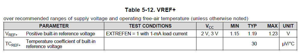
Is there any information (specs) available about the relation between the external VREF+ output (1.2V) and the internal reference voltage (1.5V) used by the MSP430FR2422 ADC?

How accurate is the coupling in absolute values, taken into account the production distribution of this device?


In our application the MSP430 VREF+ output feeds some circuitry and the output of this circuitry is sampled by the MSP430 ADC, so conversion accuracy directly depends on the degree to which these voltages are matched.


We carried out the following test to get a feel for the reference voltage couplings

Settings:

ADC positive reference voltage VREF (ADCSREFx = 001b)

ADC channel A1 (VREF+ output) (ADCSHSx = 1)

Conversion results with multiple prototype PCBs:


Serial number

Reference output VREF+ Conversion results


Min.

Max.

SN004

0x333

0x334

SN006

0x334

0x336

SN007

0x332

0x334

SN014

0x330

0x332

among all samples

0x330

0x336


I expected the min. max. results to be closer together.


We could implement a software routine which performs above measurement (ADC conversion VREF+ output) and “calibrate” our result with this value. This would be one way to increase our accuracy. Any other suggestions?

Best regards.

  • Hi Patrick,

    We do not provide a MIN/MAX value for the on-chip reference. However, we do provide some calibration value, locating at the device TLV area. You could refer to the device User's Guide for detailed information, shown as below. Also, if you want a accurate ADC, you also need to calibrate your ADC. The method of ADC calibration is right below the reference calibration chapter, shown below.

  • Hi Harry,

    We already implemented the ADC calibration method before I started this thread. There was no noticeable improvement found so I "forgot" to mention these values in the table.

    Find the ADC calibrated values in the last two columns:

    Serial number

    ADC gain factor

    ADC offset

    Reference output VREF+ Conversion results

    Raw values

    ADC calibrated values


    Min.

    Max.

    Min.

    Max.

    SN004

    0x8013

    0x0000

    819

    820

    819.47

    820.48

    SN006

    0x8009

    0x0000

    820

    822

    820.23

    822.23

    SN007

    0x8011

    0x0000

    818

    820

    818.42

    820.43

    SN014

    0x8009

    0x0000

    816

    818

    816.22

    818.22

    among all samples

    816

    822

    816.22

    822.23

    Seems to me that MSP430 reference circuitry is the root cause of this error.

    Are both references coupled? Is the VREF+ derived from the 1.5V ADC reference or are they completely independent?

    Best regards,

    Patrick

  • Hi Patrick,

    Let me summarize your case here.

    You use internal 1.5V as ADC's reference, and measure A1.1 (1.2V VREF+) pin. And also, you applied the ADC calibration at the same time. But you don't use the VREF calibration, right?

    And, you guess the 1.2V VREF+ output is derived from the 1.5V internal reference, thus a almost same conversion result is expected among different devices from your side, which you don't see it from your test. Right?

    For the 1.2V/1.5V relation, you could refer to below figure coming from the User's Guide:

    The source of the 1.2V and 1.5V is the same, however I don't expect a same voltage relation between them.

    We do have VREF+ pins MIN/MAX spec in our datasheet, but not for the 1.5V reference.

    And, may I ask if you use decouple cap at the VREF+ pins? I would suggest you to put a 1nF decouple cap at the VREF+ pin.

    Let me know your feedback.

    Regards,

    Harry

  • Hi Harry,

    You use internal 1.5V as ADC's reference, and measure A1.1 (1.2V VREF+) pin. And also, you applied the ADC calibration at the same time. But you don't use the VREF calibration, right?

    Exactly.

    I'm still used an outdated datasheet of the MPS430FR2422 (shame on me) so I didnt found the information about VREF calibration. All the more so this would not solve the issue because the issue is a relative issue and not an absolute.


    And, you guess the 1.2V VREF+ output is derived from the 1.5V internal reference, thus a almost same conversion result is expected among different devices from your side, which you don't see it from your test. Right?

    Exactly


    And, may I ask if you use decouple cap at the VREF+ pins? I would suggest you to put a 1nF decouple cap at the VREF+ pin.

    We use a 1nF decouple cap. Some time ago I did start a thread about this issue because nothing was mentioned in the datasheet about VREF+ decoupling.

    The source of the 1.2V and 1.5V is the same, however I don't expect a same voltage relation between them.

    So the relation is static but varies among different devices?

    Best regards,

    Patrick

  • Hi Patrick,

    So actually it's you who suggests us to add a description of putting 1nF decouple cap nearby the VREF+ pin. Thanks a lot for that.

    From below figure taken from the User's Guide, you can see that even though the 1.2V and 1.5V shares the same source (from the bandgap voltage generator), they don't have a exactly linear relation. From that point, I would same the relation does vary among different devices, and also among different temperature even for same device.

    All I could suggest you is to also apply the reference calibration by using the TLV data, and then do a "accurate" measurement for the VREF+ pin voltage. But just as the datasheet shows, the voltage varies among different device and really sorry but this is what we can provide by now.

    Please keep post if you have further unclear.

    Thanks a lot for all the support!

    Regards,

    Harry

**Attention** This is a public forum