Because of the Thanksgiving holiday in the U.S., TI E2E™ design support forum responses may be delayed from November 25 through December 2. Thank you for your patience.

This thread has been locked.

If you have a related question, please click the "Ask a related question" button in the top right corner. The newly created question will be automatically linked to this question.

MSP430F2618: failure of MSP430 chip InfoB Flash

Part Number: MSP430F2618

Hello,

I would like to ask about the failure of MSP430 chip Flash.

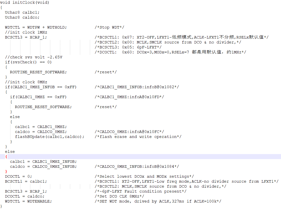
When our chip is powered on, 8MHz clock calibration information (CALBC1_8MHZ_INFOB, CALDCO_8MHZ_INFOB) is backed up in the InfoB Flash area. This calibration information was stored in InfoA (CALBC1_8MHZ, CALDCO_8MHZ). (I know this is a stupid design, but it does exist and causes problems). The clock initialization code after power on is as follows:


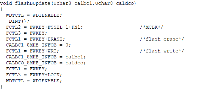
The following is the function to write flash (CALBC1_8MHZ_INFOB, CALDCO_8MHZ_INFOB).


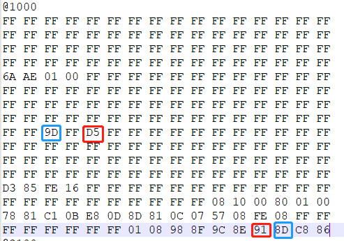
Recently, it was found that some boards (4 to 5 out of 100 boards) work abnormally. Reading flash information through BSL, CALBC1_8MHZ_INFOB, CALDCO_8MHZ_INFOB is inconsistent with CALBC1_8MHZ, CALDCO_8MHZ. There are some bit flips. The specific differences are shown in the figure below:


Now we suspect that one reason may be an error in the flash writing process, an abnormal external tooling or an abnormal power supply, which caused problems in the writing process? Or may static electricity cause problems in the subsequent storage process? However, according to the read flash data, only two flashes in the abnormal board are incorrect, which has certain regularity. So we are more suspicious that the operation of writing flash is caused by an exception, but I carefully reviewed the writing process and failed to find the exception.

Are there any irregularities in our current operations or possible errors? Or what are the possible causes of this abnormality? Thank you.

  • Hi, 

    1. I don't know why you enable the watchdog in the flashBUpdate()? 

    2. Why to disable the interruption? And There is no enable the interrupt again before flashBUpdate() return. 

    3. What is the FN1 value? As described in section 7.3.1 in user's guide slau144j, the Fftg need to be between 257KHz ~476kHz. Could you double check it? 

    Thanks, 

    Lixin 

  • Thank you for your reply.

    1. The operation of enable the watchdog in the flashBUpdate() mainly to prevent watchdog reset. But this may not be necessary because the write flash operation will not cause the watchdog to reset. We think that it should not affect the correctness of the write flash operation.

    2. The purpose of disabling interrupts is to prevent interrupts from being triggered during the flash write process and affecting the flash process. In the subsequent operation, there is an operation that enables interruption.

    3. FN1 stands for three-frequency-division. At the main frequency of 1MHz, the flash frequency is 333,3kHz, which meets the frequency requirements of 257KHz~476kHz.

  • I couldn't find the setting for the MCLK. If it is confirmed MCLK is 1MHz, the FLASH write coding seems no problem. The only concern is the erase operation. In the code example, there is a dummy write "*Flash_ptr = 0; ". But it is not seen in your code. Please try to add it and see if there is any improvement. 

    FCTL3 = FWKEY; // Clear Lock bit
    FCTL1 = FWKEY + ERASE; // Set Erase bit
    *Flash_ptr = 0; // Dummy write to erase Flash seg

    FCTL1 = FWKEY + WRT; // Set WRT bit for write operation

**Attention** This is a public forum