This thread has been locked.

If you have a related question, please click the "Ask a related question" button in the top right corner. The newly created question will be automatically linked to this question.

BOOSTXL-CAPKEYPAD: Waterproof capacitive touch-sensor does not work as expected.

Part Number: BOOSTXL-CAPKEYPAD
Other Parts Discussed in Thread: TIDM-1021, , CAPTIVATE-PGMR, MSP430FR2522

Hello everyone,

my goal is to develop a waterproof capacitive touch-sensor.

In many sources on the internet, it is said that a mutual-capacitance sensor can achieve this. 

For example, in the TI Designs: TIDM-1021 Liquid Tolerant Capacitive Touch Keypad Design application notehttps://www.ti.com/lit/ug/tidue90/tidue90.pdf?ts=1598517326899&ref_url=https%253A%252F%252Fwww.ti.com%252Ftool%252FTIDM-1021

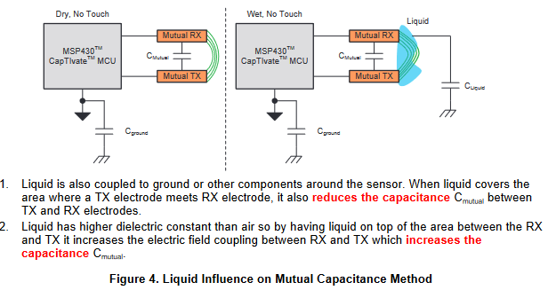
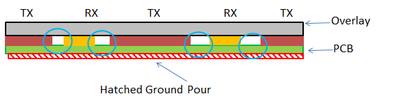
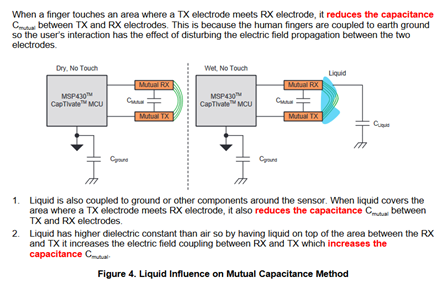
We can read page 5: "The increase of Cmutual causes the measurement result to go in the opposite direction of a touch, and this opposite result is called a "negative touch". This "negative touch" behavior helps to prevent false touch detection when liquid is present."

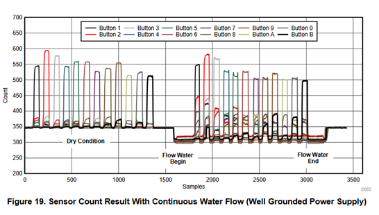
This phenomenon is also illustrated figure 19 on page 18.

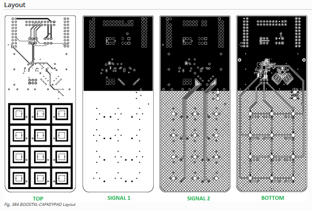
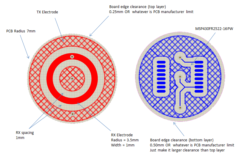
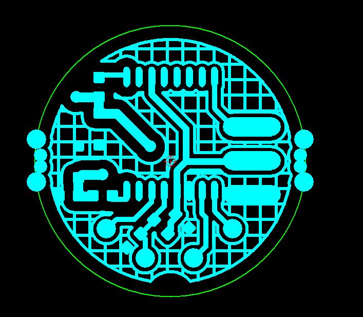
As the TIDM-1021 part is no longer available, we are using a similar part which is the BOOSTXL-CAPKEYPAD. It also works with mutual-capacitance sensing, hence we expect to achieve the same results.

However, it does not work: water on the sensor causes the mutual capacitance to decrease and hence causes the measurement result to go in the same direction of a touch. No "negative touch" is present and hence we cannot prevent false touch detection due to water.

We use the CapTIvateDesignCenter to monitor the measurement result. Here is what we get:

First we a dry touch:

And then with a water drop:

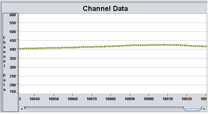
The idle state of the signal lies at the +400 level. As you can see, the effect of water drop is weaker than the effect of a dry touch, but still goes in the same direction (an increase of the measurement signal, meaning a decrease of the mutual-capacitance).

In our setup, we are using:

- the BOOSTXL-CAPKEYPAD,

- the CAPTIVATE-PGMR to program the board and monitoring signals on our computer. It also powers the board from the USB-bus.

In the application note, they also use a CAPTIVATE-ISO but it is written that if the system is powered from the host PC, there is no need for the CAPTIVATE-ISO board. So it seems OK. Our power supply is then not grounded to earth ground, but page 11 specifies that it has an influence on sensitivity only (which is not the issue in our case).

Something seems interesting on page 5: "The amount of grounding path around the sensors. Liquid couples the sensor to larger grounding path reduces the mutual capacitance and causes the measurement result to go the same direction as a touch." But I don't really understand what it means and what can we do about it.

Thank you for any help about this issue.

  • Hi Morgan,

    I am putting together a detailed response for you.

  • Hi Morgan,

    The BOOSTXL-CAPKEYPAD does use mutual capacitance as its sensing method.  The design of this PCB is focused more on limiting the effects of  conducted noise and not addressing water, hence it use of hatched ground on L2 and bottom layers, which is what you want to avoid with water.

    The design guidelines for conducted noise are completely opposite of design guidelines for moisture, which means you don't want liquids coupling to any nearby ground, either on same layer or lower layers of the PCB.  What you are seeing when you apply water is the coupling to the inner ground layers, which steals charge from the mutual electrode (same as when you touch with finger).  If you carefully apply a small drop of water only directly on one of the buttons, you should see the signal go negative or drop below the LTA.  This effect is caused by the dielectric of water improving the coupling between the RX/TX electrodes.

    For this reason, it is recommended that the PCB use individual buttons (not sharing RX lines with other buttons) and the top layer to include a hatched pour which is the single TX electrode.  Here is snippet from TIDM-1021 user's guide describing this.  This is exactly why you will not get good moisture performance with the BOOSTXL-CAPKEYPAD.  I have PCB design files and gerbers for the TIDM-1021 if you want them.

    With this design, the entire surface of the top layer becomes the TX electrode, when scanning the sensor, and grounded when not.  In this way liquid cannot couple to the ground pours on the lower layers.

  • Hello Dennis, thank you very much for these explanations.

    I have another question regarding this. We would like to achieve a small design with our sensor (we would like if possible a round PCB of radius 6-7mm).

    Hence we would like to put the microcontroller along with its few components required (a few resistors and the decoupling capacitors) on the other side of the PCB. Do you think it would be possible or would it destroy the sensor waterproof performances?

    We would for example use a 2 layer PCB with the TX and RX electrodes only on the top layer and the components on the bottom layer.

    If it is not possible, do you think we could use wires (like 10cm) to connect the electrodes to the microcontroller pins? I know it is not recommanded usually, but we do not have much space to place a bigger PCB in our system.

    BTW, in the BOOSTXL-CAPKEYPAD they are sensing IO for prototyping. We would like prototype our electrodes but we don't know how to get it works. The 3 sensing lines are connected to TX0 TX1 and TX2 which are all TX electrodes inputs. How can we connect our TX/RX electrodes ?

    Thank you very much.

  • Hi Morgan,

    Here are the sizes of possible candidates compared to the 6mm and 7mm PCB.

    The only one that I think you could possible get to fit is the (2.29x2.34)mm, DSBGA package, which will be tricky to route on only two layers and is not going to be the cheapest solution.

    Your other idea about having only the sensors on the PCB and the MCU back on a main PCB could work.  In that case I would suggest using a self capacitive sensor (single channel) with no grounds on the PCB, only the electrode.  The other option would be mutual, but is tricky.  This would require 3 wires; one for TX, one for RX and one for ground.  Although mutual measures the capacitance between the electrodes, you need some ground under the RX/TX as a reference, especially since this is floating 10cm out in space.  You also have to keep the RX and TX wires separated some distance until these signals meet on the PCB, else, just like self capacitive mode, the 10 cm of wires are potentially sensitive to hand, finger.

    The downside is the wire from the main PCB to the sensor PCB is just as susceptible and the electrode itself. Not sure what exactly your application is, but if the wire is routed such that it could detect a person's hand/finger, then you will need to provide some type of shielding in the area of potential interaction.  I don't think you need to shield the entire length of the wire.

    Another downside to using wires is noise.  You will be creating an antenna that is susceptible to electrical disturbances that could potentially couple into the wire.  If your application has a radio or switching power supply, these are 2 noise sources you will have to contend with.  Also, if you need to perform pass conducted noise and EFT/ESD testing, this probably won't work, unless you shield the entire length of the wire.  But that still leaves the electrode on the PCB susceptible to noise.

    Can you provide additional information about the intended use?

  • Thank you for your help Dennis.

    Our PCB is 6-7mm in radius so it would be like 12-14mm diameter. Hence I think we will have enough space to put an MSP430FR2522 in TSSOP-16 package (also in QFN-20, but it is easier to prototype with TSSOP-16 because we do not have the equipment to solder QFN-20 components).

    We already tried a self-capacitive sensor. It worked well when dry but it was triggerred by water drops, which is a real issue for our application. We are currently designing an human-machine interface which will be embedded on a boat. The HMI will be placed in the cabin and hence water will not flow on it. However we need to avoid any false detection caused by moisture (like moists hands or few water drops due to condensation for example). For ergonomic reasons and also for spacing reasons, we cannot design a huge PCB for the sensor. Finally, the sensor PCB will be embedded in a plastic package and sealed with synthetic resin for waterproofness. 

    I do not understand what do you mean by "you need some ground under the RX/TX as a reference". I thought we should avoid ground coupling? 

    If we use wires, I don't think it would be a problem regarding detecting a person's hand because the wires would be put in a way than a person could not approach it closer than 3 centimeters (at this range, the BOOSTXL-CAPKEYPAD electrodes are not detecting anything).

    Thank you.

  • Hi Morgan,

    My comment regarding "some ground under the RX/TX as a reference" is for a mutual capacitive sensor, not self capacitive.

    Ok, what about using a small circle as the (RX) electrode and the rest of the surface filled as the (TX) electrode?

    el

  • Hello Dennis, 

    In the design guide, we can find the following:

    http://software-dl.ti.com/msp430/msp430_public_sw/mcu/msp430/CapTIvate_Design_Center/latest/exports/docs/users_guide/html/CapTIvate_Technology_Guide_html/markdown/ch_design_guide.html#buttons

    Mutual Capacitive Button Shapes

    The electrode shape is typically rectangular with common sizes being 10mm and smaller. Ultimately, the size will depend on the required touch area. In the diagram below, the TX and RX electrodes are identified and a suggested silkscreen button outline pattern is shown. The position of the vias on the TX and RX electrodes provide flexible signal connection points when routing traces.

    • Simple Square Electrode

      • Easiest to layout

      • Highest sensitivity

      • TX on outside, RX on inside

      • For single layer designs, can open TX on one side and feed RX trace through (preferably not in a corner)

      • Better sensitivity if traces on two layers

    We would like to optimize the sensitivity because the sensor will lie behind a plastic panel of 3-5mm thickness.

    Do you think we should place TX and RX on two different layers?

    Which design would you choose between the following: (TX is in blue and RX in green):

    We can also read in the design guide:

    A good design practice is to keep the size of the button as small as possible, which minimizes the capacitance and will help with the following:

    • Reduce susceptibility to noise

    • Improve sensitivity

    • Lower power operation due to smaller capacitance and reduced electrode scan time

    Regarding this quote, is there a minimum electrode size or can we shrink it as desired? Do you recommend using the whole PCB surface for the electrode, or perhaps just decrease the RX size and filling the whole space with TX, or something else?

    Thank you.

  • Hi Morgan,

    For this application I would stick with the design shown here. It is drawn to scale (7mm radius).

    The most important design consideration here is the 3-5mm thick overlay.  To create an effective e-field that will propagate further, you want to separate the RX and TX by some distance.

    In the design guide it mentions 1/2 of the overlay thickness, but in this case that would be from 1.5mm to 3.5mm, which will eat up all your area for the TX electrode.

    I'm suggesting 1mm as a trade-off.  You should have enough sensitivity to interact through a 5mm thick overlay.

    Next, you see the hatched ground on bottom layer (blue).  I mentioned you need some ground reference for the mutual to work properly.  Although after you place your other components there may not be much area for a ground pour.  Do your best.  Also, when routing the RX and TX, keep them apart as much as possible.  I chose pins that were not next to each other on the MCU.

    Note that the ground pour on the bottom layer should be further from the edge of the PCB than the TX pour on the top layer.  This will help prevent potential coupling between moisture and the ground around the edge of the PCB.

    With respect to moisture, when the TX electrode is driven, moisture will not be able to couple to the ground on the bottom layer.  The the TX is not driven it is a ground potential.

    Of course, at the end of the day it may take an iteration or 2 to get a good balance, but I feel confident the design shown will work for you.

  • Hello Dennis, thank you very much for your help and this design.I will try to see if my mechanical engineers colleagues can provide me few more millimeters space to increase somewhat the PCB size in order to increase the TX/RX distance.

    What I would like to emphasize is that the most important parameter for us is the water-rejection behavior. Sensitivity is also important but comes just after that. I will also ask my colleagues if we can decrease a little bit the overlay thickness.

    Regarding that, what is the role of the ground pour ? Won't it decrease the water-rejection behavior?

    And when we talk about "ground pour", are we talking about the power supply ground or are we talking about the earth ground?

    Last question: will there be any advantage to route RX and TX on different layers ? For now we were talking about a 2-layers PCB but it won't be a problem for us to change for a 4-layers PCB.

    Thank you very much.

  • Hi Morgan,

    The primary role of the ground pour (from the component side) is to shield the top sensor side from possible electrical disturbances that may come from sources from behind the sensor  (don't know if you have a radio or switching power supply sitting somewhere behind the sensor).  It also provides a uniform distributed ground for the MCU and other active components.

    On a 2-layer board there is isolation between the sensor on the top side from the MCU directly underneath, so there is potential for noise from the MCU.  In your design you aren't driving LEDs or any other high currents so I'm not too concerned about it on a 2-layer PCB.  A 4-layer PCB would be optimal, with layer 3 as an internal hatched ground pour.

    The secondary role of system ground (the ground on the PCB, not earth) is to provide some amount of balanced self capacitance from the RX and TX electrodes.  This helps provide a balance in the internal biasing circuits.

    So your question about the water rejection is valid.  If you look at a cross-section of the PCB, there are regions in between the RX and TX where water can couple through the overlay and PCB to the ground pour on the backside, but the change in capacitance caused by the moisture is significantly smaller than the change of capacitance between in the RX and TX electrodes in mutual mode. Now if you imagine the TX electrode is a ground pour on the top side and you are driving the RX electrode in self capacitive mode, then you have a serious coupling issue.  See the difference?

  • Hello Dennis, thank you very much for these explanations.

    As designing a 4-layer PCB is not a problem for our application, I think we will go on this way.

    Is it better to have TX and RX on the same layer or on two different layers? If on two different layers, would it be better to have TX or RX on the top layer (and the other on layer 2)?

    If layer 3 is used as an internal hatched ground pour, should we also do an hatched ground pour on the bottom layer (the layer containing the components)?

    What is the best thing to do with the unused layer? By default, it will be a full copper pour unconnected, could it cause issues with the sensor/electrodes?

    Thank you.

  • Hi Morgan,

    We did some evaluation in the past with RX on top layer and TX on next layer down and the other way around. We found no benefit to placing RX and TX on different layers.

    If this were a more complex design with multiple RX/TX, then I would use layer 2 for routing RX/TX signal traces.  But this design is so simple you can run a signal via straight from bottom layer to the top layer practically anywhere to connect to the electrodes.  So you want to leave layer 2 empty.  No pours on this layer.  This layer is strictly a spacer layer.

    Layer 3 would be the hatched ground, preferably a 25% hatch.  If you assume a 6mil trace width that would correspond to a grid spacing of ~48mil.

    %hatch = 100 * ( 2 * (w/g) - (w/g)^2), where w = trace width, g = grid spacing.

    Layer 4 (components) you can do whatever you want on this layer in terms of ground.

  • Thank you very much Dennis for your help, this is totally clear to me now.

    I will give you feedbacks when the sensor is built. Thank you.

  • Hi Morgan,

    That sounds good.  In the meantime I'm going to mark this as resolved.

    Later you can either come back click the "This did NOT resolve my issue" button and reply to this thread with more information.
    If this thread locks, please click the "Ask a related question" button and in the new thread describe your results.

    Good luck ;)

  • Hello Dennis, as promised I give you a feedback of our design.

    We have built the touch sensor, but using only a 2-layers PCB because our supplier could not build a 4-layer PCB with the schedule we asked him.

    One layer is the electrode you suggested, the other layer is the component layer with a ground plane 25% hatched and with an higher board clearance as requested.

    Here is our design:

    We are facing problems with water. Water increases the mutual capacitance as mesured by the sensor, instead of decreasing it. Hence we do not observe the "negative touch" expected.

    I do not understand where does the problem come from. Can you help us to understand it ? Thank you.

  • Hi Morgan,

    Yes, this is completely expected.

    From the TIDM-1021 Moisture reference design, it describes this in note (2) below

    Here are some test results from TIDM-1021 showing the influence of flowing water on the touch.  As you can see, the count and LTA go lower when water is present.

    Referring to note (2) above, this is due to the capacitance water adds across the RX/TX electrodes (same affect if sensor was self cap and you touch with finger), but notice the "delta" values still go to higher counts during a touch (as expected for a mutual capacitive sensor).

    What you may need to do in your application code is monitor if the baseline goes shifts lower and during this time temporarily change the touch threshold.  This isn't always the case though.

    Try logging your sensors response to water and touch as done above.  Then either post the plot or provide me the .csv file.

    There is a logging button next to the "Connected" button in the sensor view.  The data is stored in the same directory as the captivate design center project you are using.

  • Hi Morgan,

    It's been a few days since I have heard from you so I’m assuming you are making progress.

    I'm going to mark this thread resolved for now.
    If this isn’t the case, please click the "This did NOT resolve my issue" button and reply to this thread with more information.
    If this thread locks, please click the "Ask a related question" button and in the new thread describe the current status of your issue and any additional details you may have to assist us in helping to solve your issues.


**Attention** This is a public forum