This thread has been locked.

If you have a related question, please click the "Ask a related question" button in the top right corner. The newly created question will be automatically linked to this question.

TIDM-1021: About single-sided mounting

Genius 5840 points
Part Number: TIDM-1021

Hello.

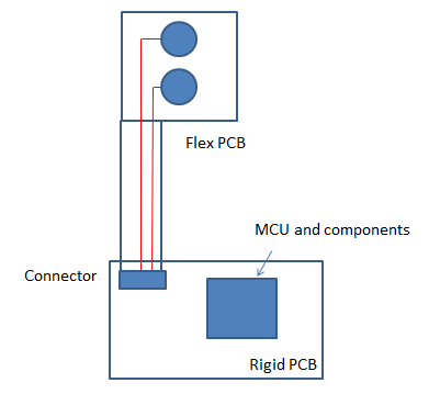
I am evaluating TIDM-1021 board and interested in liquid-tolerant touch.

But the board is double sided mounting.

Are there any way to mount to single-sided board and realize liquid-tolerant touch?

I would like to use flexible sensor sheet for electrode. 

Regards,

U-SK

  • Hello U-SK,

    The PCB is double sided because the electrodes (sensors) are on one side and components are on the other side.

    I think you are asking is it possible to create sensors on a flex-pcb.  Yes.  The flex pcb can be only sensors and have a tail with connections to another PCB where the MSP430 CapTIvate MCU could be located.

  • Hi Dennis,

    Thank you for your reply.

    I would like to design the sensor electrode using transparent material (ex. PEDOT) and flexible PCB.

    But almost flex-pcb manufacturer supports single sided layout.

    So I woulld like to make liquid tolerant touch board using single sided flex-PCBs.

    I am considering following measures.

    1.Separate each single-sided sheet with TX electrode and RX electrode, and put PET material in between and stick them together.

     (If necessary, attach the GND sheet to the back side.)

    2.Implemet both the TX and RX electrodes on one side. Hatch the TX electrode so as to avoid tracing from the RX electrode to the MCU.

     (If necessary, attach the GND sheet to the back side.)

    Can it be achieved with the above?
    Do you have any concerns?

    Is there a solution to achieve TIDM-1021 with a single-sided flex-pcb?

     Regards,

    U-SK

  • I'm not familar wth PETDOT, although I see it is a flexible conductive material.

    Here is my suggestion.   Please feel free to draw what you are thinking.

  • Hi Dennis,

    Thank you for your reply.

    PEDOT can be used as  flexible and biodegradable thermoelectric generators as follows.

    I would like you to tell me about Flex PCB side you figured.

    If flex PCB can be printed only single sided, I am considering following way using 2 transparent flex PCB sheets.

    If transparent flex PCB can be printed double-sided and can't be placed the through holes, I am considering following way using only one sheet.

    The RX electrode and the GND area at RX electrode position should be transparent to allow LED light to pass through.

    Can we achieve liquid tolerant touch like TIDEM-1021 taking above measures?  

    Are there any concerns?

    Regards,

    U-SK

  • Hi U-SK,

    Yes, either one of these designs will work.

  • Hi Dennis,

    Thank you for your reply.

    When looking at TIDM-1021, RX traces is hidden behind the board and just above the front seems to be hatched with TX.

    My idea's concern is that the RX trace will be exposed on the touch surface and will falsely detect if we touch to other area than a button.

    Is it ok in above situation?

    If we perform double-sided printing on a transparent flex-PCB as described above, the transparent flex-PCB is so thin that the GND hatch surface and the electrode surface are extremely close together.

    In CapTIvate technology Guide, PCB thickness seems to be recommended as large as possible.

    So I am thinking of making a space between the electrode surface and the GND hatch surface as shown below.

    For example, when acrylic is sandwiched between them, the dielectric constant is different from FR-4.

    How thick is desirable?

    Is it possible to check the created Gerber data with a private message?

    Best Regards,

    U-SK

  • Hi Dennis,

    Do you have any updates?

    It's urgent project, so I would appreciate it if you could reply as soon as possible.

    Thank you for your cooperation.

    Regards,

    U-SK

  • Hi U-SK,

    Regarding the RX traces and sensitivity to touch, yes, this is very possible.  On regular FR4 the traces can be routed on bottom layer, safely away from the surface.  In your design you won't be able to do that, so I would suggest leaving a large space between the TX hatched fill and the traces leading up to the RX pad.

    Regarding an overlay, you never want to expose any electrode (RX or TX) to the environment. The overlay is an important part of the capacitive touch system.  It protects the electrodes from moisture and potential ESD.  For mutual capacitance sensors, it also prevents a finger from "shorting" out the capacitance between the TX and RX electrode.

    Yes, you can send private message to include gerbers.

  • Hi Dennis,

    Than you for your reply.

    Firstly, I sand friend ship to you.

    Could you please confirm it?

    Although not shown in the figure below, I will prepare PET as an overlay separately and cover it.

    So Acrylic described above is used for spacing between GND hatched surface and Electrodes surface.

    Because CapTIvate Technology Guide describes as follows.

     H gets smaller, the parasitic capacitance increases, which results in a decrease in sensitivity. In most applications, a two-layer PCB is used, and a standard FR4 PCB with the thickness of 1 mm to 1.6 mm is recommended.


    So I think that acrylic is also necessary to obtain high sensitivity with a certain thickness such as 1 to 1.6 mm.

    But Acrylic and FR-4 is different from dielectric constant, how thick do you think acrylic needs?

    Regards,

    U-SK

  • Hi Dennis,

    Do you have any updates on my question?

    And I would also appreciate it if you approve my "Friend-Request" in order to start discussion via private message.

    Regards,

    U-SK

  • Hi U-SK,

    I have accepted your friend request.

    Regarding your question, yes, the more space between the ground on the bottom layer and the electrode on the top layer, the higher the sensitivity.

    This is particularly true for self cap designs, not so much for mutual.  Mutual, which is what you are attempting measures the capacitive changes between the RX and TX electrodes and not affected to much by the ground underneath.

    The dielectric of the material doesn't matter in this case.  If you are familiar with flex PCB construction and stackup you see it is possible to have the layers close together, but you must be careful with the density of the ground pour fill under the sensors. 

    Try to send me your files privately.

  • Hi Dennis,

    Thank you for your reply.

    Let me proceed with the more detail discussion with a private message.

    Regards,

    U-SK 

**Attention** This is a public forum