This thread has been locked.

If you have a related question, please click the "Ask a related question" button in the top right corner. The newly created question will be automatically linked to this question.

MSP430F67641A: Could not set core voltage to its intended 3V

Part Number: MSP430F67641A
Other Parts Discussed in Thread: MSP430WARE, MSP430F6736, MSP-TS430PZ100B

Dear Team,

We are designing a poly-phase energy meter and its purely a customised design from your evaluation module. The core part of the circuit remains the same (voltage,current measurement, pin mappings) as it is, but just the output's (display, external communications) were altered.

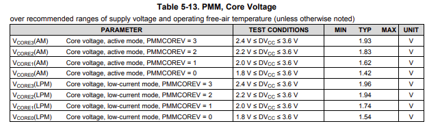
I could get our prototype working, but however i see some troubles with the core voltage. From your sample code i use the below to set the core volltage to 3V, but still see the voltage on (Pin-23 VCORE) is always 1.8V limiting the crystal to 8Mhz. (Controller is powered with 3.3V)

This is the below code that i have picked from your samples. Could you please me if i am missing something ?. Or is the core voltage dependant on some Aux power supply's which we don't focus on at the moment.

Note: At the moment we dont use any Aux supply's and the external 32khz crystal is not mount and left open.

     - AuxVCC1&2 are capped to ground

     - DVSYS (20&74) connected and capped to ground

     - AuxVCC3 left open and external 32khz crystal not mount

void System_Init()

{

PMMCTL0_H = PMMPW_H;
SVSMHCTL&=~SVSMHRRL_7;
SVSMHCTL|=SVSMHRRL_4;
AUX3CHCTL = AUXCHKEY | AUXCHEN | AUXCHC_1 | AUXCHV_1;
AUXCTL0 = AUXKEY;
AUXADCCTL = AUXADC | AUXADCSEL_0 | AUXADCR_0;
AUXCTL2 |=AUX0LVL_6 +AUX1LVL_5 + AUX2LVL_5;
AUXIE |= (AUX0SWIE | AUX1SWIE | AUX2SWIE | AUXSWGIE | AUX0DRPIE | AUX1DRPIE | AUX2DRPIE | AUXMONIE );
PMMCTL0_H = 0;

SetVCore(3);
__bis_SR_register(SCG0); /* Disable the FLL control loop */
UCSCTL6 = (UCSCTL6 | XT1DRIVE_3); /* Highest drive setting for XT1 startup */
while (SFRIFG1 & OFIFG)
{
/* Check OFIFG fault flag */
UCSCTL7 &= ~(DCOFFG | XT1LFOFFG | XT2OFFG); /* Clear OSC fault flags */
SFRIFG1 &= ~OFIFG; /* Clear OFIFG fault flag */
}
UCSCTL6 = (UCSCTL6 & ~(XT1DRIVE_3)); /* Reduce drive to something weaker */

UCSCTL0 = 0;
UCSCTL1 = DCORSEL_6; /* Set RSELx for DCO = 25MHz */
UCSCTL2 = FLLD__4;
UCSCTL2 |= (192 - 1); /* Set DCO Multiplier for 25MHz */
/* Set FLL to 32768*4*192 => 25165824Hz */
__bic_SR_register(SCG0); /* Enable the FLL control loop */

UCSCTL5 |= DIVS__1 | DIVA__32;
UCSCTL4 = SELM__DCOCLK | SELS__DCOCLK | SELA__XT1CLK; /* 24MHz MCLK, 24MHz SMCLK, ACLK (25Mhz/32)*/

__delay_cycles(100);

}

Question-2: Do you have a complete working sample code for the energy meter (https://www.ti.com/tool/EVM430-F67641) ?.

I could access its schematic, but could not directly get the complete working project. i got pieces of code and its too hard to put it together to have a compilable code.

Thanks in advance,

Surya

  • VCore is regulated core power supply output with related capacitor on device VCore pin. Maximum value for VCore is 3 (it is just number value, not volts) and with this maximum value and 3.3V supply device should work on 25 MHz (check device datasheet because some devices from f5xx/6xx family are limited to 20MHz). Voltage on VCore pin is close to 2V (not 3V).

    VCore voltage should be increased in steps, one by one, until max value is reached, so check this function SetVCore to find it, if this is already included inside.

  • From your sample code i use the below to set the core volltage to 3V, but still see the voltage on (Pin-23 VCORE) is always 1.8V limiting the crystal to 8Mhz.

    The MSP430F67641A datasheet gives the typical voltage on the VCORE pin at different PMMCOREV settings:

    As the datasheet only gives typical values, measuring VCORE = 1.8V for PMMCOREV = 3 isn't necessarily a problem.

  • SetVCore(3);

    Looking at MSP430Ware 3.80.13.03 the SetVCore function is implemented as a while loop which increments the PMMCOREV setting one step at time, and the reset value of PMMCOREV is zero.

    While the datasheet only gives the typical value for the VCORE voltage, if you monitor the VCORE voltage as step the SetVCore function in the debugger you should be able to check if the VCORE voltage increments at each step to confirm the SetVCore function is having an effect.

  • Dear All,

    Thanks a lot for your replies. That really made my understanding clear on the core voltage level and that should be fine in my prototype.

    Question-1: My most concern out of it was that, using the same code mentioned above to set the crystal to 25Mhz was not working and the clock is forced to 8Mhz. Are there any dependencies if i have to work with the full 25Mhz capacity ?

  • My most concern out of it was that, using the same code mentioned above to set the crystal to 25Mhz was not working and the clock is forced to 8Mhz.

    Can you clarify what is forcing the clock to 8MHz?

    Also, the code in the first post is attempting to start XT1, but it was also mentioned that:

    external 32khz crystal is not mount and left open

    Can you clarify what is connected to the XIN / XOUT pins?

  • Thanks again for your quick reply.

    The Xin/Xout pins are left open unmount. 

    Can you clarify what is forcing the clock to 8MHz?

    I am not exactly sure what is forcing the clock to 8. I wanted my application to run at 25Mhz and i use the below code. When i use this code, the maximum clock i could achieve its 8Mhz for some unknown reasons (checked with __delay_cycles). Could you please help if i am using the right code to configure the clock to run at 25Mhz ?

    SetVCore(3);
    __bis_SR_register(SCG0); /* Disable the FLL control loop */
    UCSCTL6 = (UCSCTL6 | XT1DRIVE_3); /* Highest drive setting for XT1 startup */
    while (SFRIFG1 & OFIFG)
    {
    /* Check OFIFG fault flag */
    UCSCTL7 &= ~(DCOFFG | XT1LFOFFG | XT2OFFG); /* Clear OSC fault flags */
    SFRIFG1 &= ~OFIFG; /* Clear OFIFG fault flag */
    }
    UCSCTL6 = (UCSCTL6 & ~(XT1DRIVE_3)); /* Reduce drive to something weaker */

    UCSCTL0 = 0;
    UCSCTL1 = DCORSEL_6; /* Set RSELx for DCO = 25MHz */
    UCSCTL2 = FLLD__4;
    UCSCTL2 |= (192 - 1); /* Set DCO Multiplier for 25MHz */
    /* Set FLL to 32768*4*192 => 25165824Hz */
    __bic_SR_register(SCG0); /* Enable the FLL control loop */

    UCSCTL5 |= DIVS__1 | DIVA__32;
    UCSCTL4 = SELM__DCOCLK | SELS__DCOCLK | SELA__XT1CLK; /* 24MHz MCLK, 24MHz SMCLK, ACLK (25Mhz/32)*/

    __delay_cycles(100);

    I tried to add this part of code form the sample program since the crystal was force limited to 8Mhz like mentioned. Having this part of code or not resulted in the same clock result. This was just a blind try from my side!.

    PMMCTL0_H = PMMPW_H;
    SVSMHCTL&=~SVSMHRRL_7;
    SVSMHCTL|=SVSMHRRL_4;
    AUX3CHCTL = AUXCHKEY | AUXCHEN | AUXCHC_1 | AUXCHV_1;
    AUXCTL0 = AUXKEY;
    AUXADCCTL = AUXADC | AUXADCSEL_0 | AUXADCR_0;
    AUXCTL2 |=AUX0LVL_6 +AUX1LVL_5 + AUX2LVL_5;
    AUXIE |= (AUX0SWIE | AUX1SWIE | AUX2SWIE | AUXSWGIE | AUX0DRPIE | AUX1DRPIE | AUX2DRPIE | AUXMONIE );
    PMMCTL0_H = 0;
  • Could you please help if i am using the right code to configure the clock to run at 25Mhz ?

    The attached project for a MSP430F6736 is based upon driverlib, and sets a 25MHz clock using REFO as the FLL clock source.

    Ran on a MSP-TS430PZ100B which has no XT1 crystal fitted, and the AuxVCC1,2&3 supplies were left often.

    The program toggles P1.0 every 1,000,000 clocks. An LSA showed that the CPU frequency was ~24.86 MHz which is within the expected range considering REFO has a ±1.5% tolerance at room temperature:

    ucs_ex1_DCO25MHz.zip

    I am not exactly sure what is forcing the clock to 8. I wanted my application to run at 25Mhz and i use the below code.

    I tried your code fragment, and if stepped in the debugger then got stuck in the loop which attempts to clear the oscillator fault flag. The posted code fragment is not writing to UCSCTL3, and the reset value of UCSCTL3 selects XT1CLK as the FLL clock source. While the user guide suggests the UCS Module Fail-Safe Operation should cause REFO to be automatically selected as the reference source into the FLL in the event of crystal fault maybe that is no happening for some reason.

    If there is no crystal fitted, probably more reliable to explicitly select REFO as the FLL reference source.

  • Thank a lot for your support!. That was really quick that i got the issue resolved in 1 day from you.

    I am able to now get the device running at full clock 24Mhz from your example.

    I would like to appreciate your efforts to exactly replicate my scenario and provide the right suggestion too early. This kind of support we get from you is the main reason we always look for texas parts first in the market!.

    Great job, and thanks again for your quick support.

**Attention** This is a public forum