This thread has been locked.

If you have a related question, please click the "Ask a related question" button in the top right corner. The newly created question will be automatically linked to this question.

TIDA-00879 ISSUE

Other Parts Discussed in Thread: TIDA-00879, MSP430F6736

HI

I have some doubts on the TI design TIDA-00879. Please help.

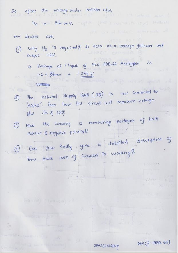
Please see the following pictures:

  • Hi Susan,

    I am trying to raise this post to the attention of the TIDA-00879 author so that they can properly address your questions.

    Regards,
    Ryan
  • Hi Susan,

    In response to your questions, U3 serves as a buffer for the R6/R8 100 Kohm resistor divider to drive the 200K (typ) SD24_B input impedance and establishes V+ as a 1.2V common mode reference voltage for the system. This output also serves as the reference voltage potential for the applied external voltage being measured (i.e. J6 is used as the reference point between the TIDA-00879 and external system, not J8). Therefore, the voltage at the positive input of the MCU SD24_B analog pin is a constant 1.2V, independent of the external voltage being measured. The 54 mV you calculate in your example represents the delta voltage between the V+ and V- inputs, so the voltage at the negative input of the MCU SD24_B analog pin in your example is 1.146V. If an external voltage of -60V is applied, V- will be 1.254V while V+ is still maintained at 1.2V, thereby creating a V+/V- delta voltage of -54 mV. In either case, the common mode voltage requirements specified in the MSP430F6736 datasheet are maintained. This +/- 54mV is then gained up by the SD24_B PGA by a factor of 16 as described in the TIDA-00879 design guide before being input to the ADC.

    Hope this answers your questions.

    Regards,
    Russ

**Attention** This is a public forum