This thread has been locked.

If you have a related question, please click the "Ask a related question" button in the top right corner. The newly created question will be automatically linked to this question.

MSP-CAPT-FR2633: Capacitive Touch pad Design

Part Number: MSP-CAPT-FR2633

Hi,

I am currently using the CapTIvate design guide to design my own capacitive touch PCB. It is indicated in the design guide that the digital LED signals should always be at least 4 mm from the capacitive touch pads and tracks. Though it seems unclear whether the 4mm rule applies to just tracks on the same layer or also if tracks are on a different layer.

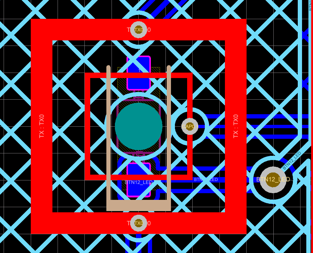
Currently my design is what is in the image it is 2 layers right now (red and green are the tracks). I am thinking of just putting the LED on a separate 3rd layer. Would this be enough to to ensure it operating as it should. As can be seen the LED is currently going to be directly below the touch pad (green), however this is needed due to size constraints. Also even with the 3rd layer I will have tracks running to the capacitor  but they will likely go within a millimetre of the capacitive touch traces but on a separate layer, will this cause any problems?

Thanks for your advice!

  • Hi Dylan,

    While it it is ideal to have a few mm of spacing between digital signals and the touch sensing electrodes, in some cases this is not feasible because of design constraints.  LED backlighting is a good example of a case where the best practices are "bent" a little.  What you are showing in your layout is a very common usage of LEDs, and I would not expect any problems here.

    The guidelines are designed to reduce the overall coupling between switching nodes and the electrodes.  The most sensitive nets to noise are going to be the RX nets.  We have done quite a few designs with reverse-mount LEDs mounted in just this way (inside of a mutual capacitance button).  The LED has to come into close proximity with the electrode in order to be properly positioned for backlighting.  To minimize further routing, it is a good idea to provide some separation between your RX routing and the LED drive lines, if the traces run for great lengths nearby each other.  If you do add an additional layer, this will give you some flexibility and is recommended.  It would allow you to add a ground plane or ground hatch, which can lower crosstalk and improve noise immunity.

    Below is an example of an LED inside of a button much like yours.  This is a 4-layer PCB, with the sensor on the top, a void on layer 2 (directly beneath the sensor), a ground hatch on layer 3 with some routing, and a VCC hatch on layer 4 along with some routing.  It is possible to do this with just two layers, but it is more difficult.

    Are you going to be applying a PWM signal to these LEDs, or are they static (on or off only)?  If your LED's are static, you really don't have much to worry about.  Even with PWM, usually the PWM frequency is well below the CapTIvate acquisition frequency, and there is not any interference.  Where you tend to see interference more is if you route a high speed SPI communication line next to an RX for a decent length, and then run that SPI at a frequency close to the CapTIvate operating frequency.  As mentioned earlier, I do not have any concerns with your LED placement.

    Regards,
    Walter

  • Hi Walter,

    Thanks for the excellent reply! To answer your question about whether my LEDs are using PWM or are static; I will be driving the LEDs using chralieplexing. This means that there will be quick switching on the LEDs (though likely no higher than 100Hz). Since there is a high impedance state from this method I am planning to add capacitors as is recommended in the design guide.

    Also in terms of the routing, I am now thinking of doing 4 layers, with the sensors, then a ground layer, and then 2 layers with routing (one could have ground hatch as well). I assume what is most important is just that the ground hatch is preferably between the sensors and layers with routing that carry signals. Also for the Rx and Tx routing, looking at your image I see you have them on the furthest layer from sensors (buttons), which I assume is because it makes it leas likely to get and unwanted detection of touch from someone putting there finger over the Rx and Tx lines.

    Thanks,
    Dylan
  • Dylan,

    100 Hz switching will not be a problem here; this approach is fine. You are correct on adding the caps as recommended for the High-Z state.

    You are correct as well about the routing- we try to isolate RX/TX trace routing as much as possible from the user to minimize the potential for any crosstalk. A good practice is to keep your RX's routed together and your TX's routed together, and avoid bringing RX's near TX's. If you must bring them together or cross them, do so in an area that is shielded with ground. In the mutual mode, anywhere an RX and TX come together, a touch sensitive region is created.

    Walter

**Attention** This is a public forum