This thread has been locked.

If you have a related question, please click the "Ask a related question" button in the top right corner. The newly created question will be automatically linked to this question.

MSP430FR2633: CapTIvate layout query

Part Number: MSP430FR2633

Hi,

I have a potential CapTIvate customer.

They are planning to use ~20 buttons on one PCB, so FR2633 with mutual buttons is an option.

According to design guide, each button is placed side-by-side.
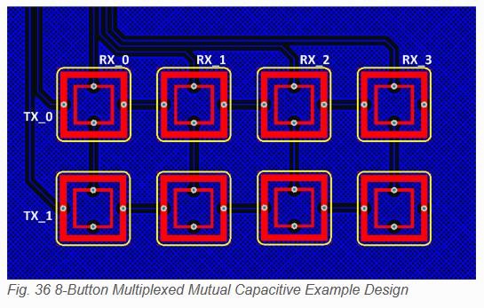

Customer is thinking to distribute these buttons equally on a big PCB (around 50cm x 10cm).

Do we need special consideration in layout in case buttons are separated on bigger PCB?

Thanks and regards,

KoT

  • Thank you for posting this question.

    The illustration shown is a simple example that represents what might be used for a simple keypad or similar.

    Buttons can be distributed as far apart from each other as needed.

    There are, however, a couple of guidelines with respect to mutual capacitive sensors and their routing traces and dimensions.  This information is available in the CapTIvate design documentation.

    I will address the most important ones here:

    1. A mutual capacitive button electrode width and spacing is very important for optimal performance.  See the recommended dimensions in the illustration.  Buttons that are made smaller or larger than 10mm should maintain a 1mm TX width and 0.5mm RX width and 0.5 spacing.

    2. The buttons can be round or square (most typical) and should be between 8 to 12 mm (10mm is typical) in diameter.

    3. When routing traces from the buttons to a connector or directly to the MCU, keep RX traces separate from TX traces, especially if they are long parallel traces.  Ok if Rx traces are close to other RX traces, and ok if TX traces are close to other TX traces.  If RX trace must run near TX trace, separate with ground trace/pour.  Ok if RX trace on one layer cross TX on another layer, but only at 90 deg.

    4. For general shielding and EMC considerations, a ground plane maybe used on one or more layers.  A 25% "hatched" ground pour provides adequate shielding on layers below and on same layer as buttons.  In most cases, it is ok to fill hatched ground, same size as button, directly underneath button.  In cases where the mechanical stackup will be >2-3mm, sensitivity may be an issue and therefore do not provide hatched ground directly underneath button.  Spacing between the ground pour on the same layer as the button as well as the traces between the buttons and the MCU are described next.

    5. RX and TX traces can be affected by parasitic capacitances in nearby grounds or ground pours on PCB layers.  If ground pour is near RX or TX trace, maintain space between trace and ground = 1/2 width of the overlay.  Example, if overlay is 2mm, then use 1mm space between trace and ground pour.

    6. Provide enough space between buttons to minimize cross-coupling between buttons.  Typically the width of one finger. The larger, the better.  For the application mentioned in this thread, this should not be an issue.

    Please ask for more information if this is not clear.

  • Hi Dennis,

    Thanks for your detailed answers!

    I need more clarification for below comment.

    In cases where the mechanical stackup will be >2-3mm, sensitivity may be an issue and therefore do not provide hatched ground directly underneath button. 

    What the “mechanical stackup” exactly means here ?
    In design guide, stackup includes decal, overlay, adhesive, copper and FR4.
    If overlay is more than 2-3mm, the hatched ground directly underneath button should not be used?

    Thanks and regards,
    KoT


  • Hi KoT,

    The mechanical stackup refers to material and spacing between the electrode and the surface area where a person's finger comes in contact with the product.

    The illustration above shows a "typical" stack would be.  Starting from the electrode (copper on top side of pcb) you have an adhesive layer an overlay and possibly a label or decal.  What is of concern is the overall thickness and the dielectric of the material.  In most cases, the adhesive layer and decal can be ignored as these are usually very thin.  What dominates is the thickness of the overlay and is recommended to be 2-3mm. The overlay material is usually some type of plastic with typical dielectrics somewhere between 3 to 4.  The material's dielectric helps propagate the e-field from the electrode to the surface where a finger comes into contact.

    For some designs, the overlay and pcb cannot be affixed together and there is an air gap due to the design of the product's enclosure.  This should be avoided whenever possible.  Since the dielectric of air is 1, this greatly attenuates the e-field that must pass through the air gap then through the overlay.  One method is to fill the gap with same material as the overlay to bridge the air gap between the electrode and the overlay.  

    Example: Overlay is 2mm, air gap is 1mm.  Fill air gap over each button electrode with material same as overlay.  Now mechanical stack up consists of 3mm of similar material, and no air gap.

    Here is a diagram illustrating the two scenarios:

    Can you describe what your stack up will be?

    Also, whether you need a hatched ground under the electrode will really be determined if conducted noise is a concern.  Can you tell me what the application is and if it is a battery powered or line powered application?

  • Hi KoT,

    I'm going to close this thread since it has been a few days since your last response and don't have any further questions.
    If this is not the case and you need additional help, you can re-open this same thread.
  • Hi Dennis,

    Yes, we can close this thread. Thanks again for your support on this.
    Sorry for my late response.

    Thanks and regards,
    KoT

**Attention** This is a public forum