This thread has been locked.

If you have a related question, please click the "Ask a related question" button in the top right corner. The newly created question will be automatically linked to this question.

MSP430FR6922: problem setting the fork crystal oscillator correctly

Expert 6310 points
Part Number: MSP430FR6922

Team,

we have problems with fork crystal for MSP430FR6922. We need to set 8MHz for MCLK and set fork external crystal to ACLK.

Below you can see the function we use, If we use it, MSP430FR6922 stays in loop do - while for a few seconds. That time is random, ranging between 1 sec and infinity.

Parameters of crystal are:

  • Package: 3215
  • Load capacitance: 6pF
  • Frequency: 32768 Hz

Can you please advise what's the issue, or where's a mistake in the code?

One remark is that if we work with msp430fr6922 on jtag programmer, described problem will not happen. If we unplug this and connect to 3V source, described problem will begin.

Thank you for your help.

TI Customer


void ClocksStart(void)

{

    PJSEL0 |= BIT4 | BIT5;                    // Enable clock function pin for crystal.

    // Disable the GPIO power-on default high-impedance mode to activate

    // previously configured port settings

    PM5CTL0 &=~LOCKLPM5;


    SFRIE1 &=~ OFIE;    //Block interrupts that occur when a crystal error occurs
    // Setup Clocks

    CSCTL0_H = CSKEY >> 8;                    // Unlock CS registers

    CSCTL1 = DCOFSEL_6;                       // DCORSEL = 0 a

DCOFSEL=6 (DCOFSEL=110)-> 8MHz

    CSCTL4 &= ~ LFXTDRIVE_2;                  // Set the power to the crystal, LFXTDRIVE 00 - 3,5 pF, LFXTDRIVE 01 - 6 pF,LFXTDRIVE 10 - 9 pF, LFXTDRIVE 11 - 12 pF

    CSCTL2 = SELA__LFXTCLK | SELS__DCOCLK | SELM__DCOCLK; // set ACLK = XT1; MCLK = DCO

    CSCTL3 = DIVA__1 | DIVS__1 | DIVM__1;     // Set all dividers to 1

    CSCTL4 &= ~LFXTOFF;                       // Enable crystal.

    P9DIR |= BIT5;

    do

    {

        P9OUT ^= BIT5;

      CSCTL5 &= ~LFXTOFFG;                    // Clear XT1 fault flag


      SFRIFG1 &= ~OFIFG;


    } while (SFRIFG1 & OFIFG);                // Test oscillator fault flag

    CSCTL0_H = 0;                             // Lock CS registers


    SFRIE1 |= OFIE;     //Allow interrupt that occurs when a crystal error occurs }

  • Bartosz,
    what crystal do you use? (datasheet) Which ESR does the crystal have and which cap does it require.
    Do you have considered the LFO Apps note with respect to parastics, cross talk in the layout?

    Please consider this oscillator is runnig with some 100nA so each disturbance or incorrect loading has an influence.

    www.ti.com/lit/an/slaa322c/slaa322c.pdf
  • Hi Dietmar,

    thanks for your feedback. We are waiting for the full datasheet of the crystal from the manufacturer.

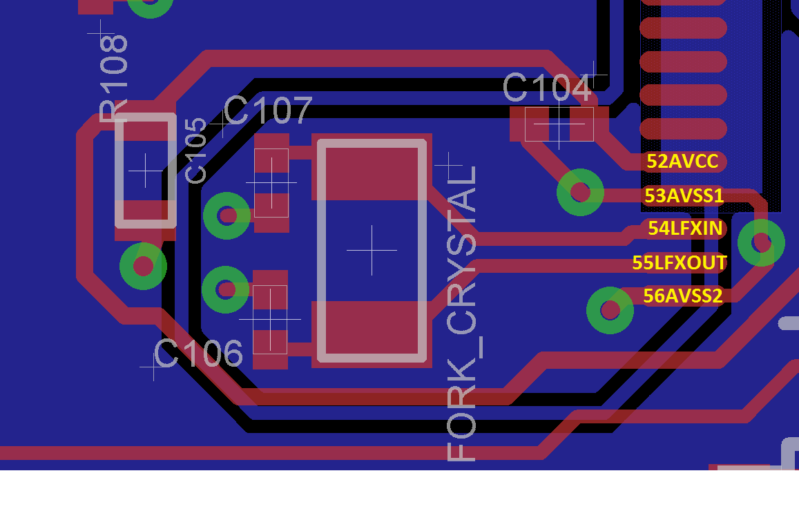
    We followed the rules of the LFO Apps note - can you check if the below layout design is fine?

    Also, we have additional two questions:

    1) Could you confirm if the function shared above for starting both clocks is fine (MCLK 8MHz, ACLK 32768 Hz)?

    2) We use msp430fr6922 in 56pin DGG Package.

    a) Can I measure precision of LFXT(10ppm) on PJ.2 ACLK(pin26) with another device?

    b) Is output signal wired directly from ACLK, or changes on pin are synchronized with MCLK?

    If changes on pin are directly from ACLK, I think that precision of LFXT can be measured.
    If changes on pin are synchronized by MCLK, precision of LFXT can´t be measured.

    Thank you,
    TI Customer

  • Hi Bartosz,

    regarding layout:
    - symetric load caps is good
    - short traces is good
    - GND island connected to local GND to reduce return current is good
    - the AVCC trace around the GND island makes not real sense to me I would have this routed behind the pins to not have the loop
    But I hink this shoud not tremendously influnce the crystal here except you have high swtiching noise on AVCC.

    regarding code:
    - code looks good maybe you can try code example msp430fr6x7x_cs_03.c from product page to check if this works and we have not overseen something
    - I would also try to not reduce drive strenths maybe the crystal has high ESR and needs more current
    - maybe clearing the HFXTOFFG as well in the loop ensuring it is not set ( I know it should not but give a trial)
    - I would take of the port toggle of P9.5 in the loop depending on your layout this might disturb the crystal during start

    regarding measurement
    - yes you can measure LFXT at PJ.2 but if the OFIFG is not you will measure the REFO there because this is the fail safe clock
    - again ACLK is switched to the pin if you set the corresponding 2nd function on PJ.2 but as long as OFIFG is set LFXT clock is not switched to ACLK but the fail safe clock
    - finally you can measure the LFXT accuaracy on the ACLK pin this is not syncd with MCLK

  • Hi Dietmar,

    thanks a lot for your feedback, it helps.

    One last thing, could you advise which of our two versions of layout would be better (attached below zip)?

    The two solutions differ by a small GND bridge (2nd solution), which is marked by an orange square.

    Thank you!

    layout.zip

  • Hi Bartosz,
    I think the 2nd solution is closer to the recommendations shown in figure 7 and 8 of the LFO Apps note.

**Attention** This is a public forum