This thread has been locked.

If you have a related question, please click the "Ask a related question" button in the top right corner. The newly created question will be automatically linked to this question.

MSP430FR5969: LPM after employing DMA

Part Number: MSP430FR5969

Dear colleagues,

I'm using the ADC embedded into the MSP430FR5969 operating at low frequency in LPM3.

Then I'm trying to transfer the result of the conversion via DMA to a given memory position.

However, I have a problem with the resulting LPM after employing the DMA.

I thought that the MCU would get back to LPM3 after transferring the data, but it stays in LPM0.

Is that what we should expect or I'm doing something wrong in the configuration?

Many thanks in advance,

Ferran

  • Ferran,

    Please give me some time to look into this further but in the meantime could you please provide a stripped down version of your project that isolates the ADC, DMA, and LPM functionality so that I can try to recreate your issue on my test setup?

    Best regards,

    Matt
  • Dear Matt,

    Thanks for your response!!

    Next, you can find the code I'm using to set the ADC, timer and DMA.

    Any feedback you have, sure it helps!!

      // CONFIGURATION OF THE ADC AT LF
      ADC12CTL0 = 0x0010; // S&H: 4 clk
                                    // ADC on
      ADC12CTL1 = 0x060C;    // 32 kHz
                                        // Repeated single channel
                                        // Clk source: ACLK
                                        // SAMPCON signal is sourced from the sampling timer
                                      // It is triggered by the timer
      ADC12CTL2=0x0011; // Conversion of 10 bits
                                  // Low power mode of the ADC enabled

                                    // Register related to ADC12MEM0:
      ADC12MCTL0 = 0x0082;    // A2 ADC input select
                                        // Voltage reference is Vcc

      ADC12CTL0 |= ADC12ENC;  // ADC enabled

      // CONFIGURATION OF THE Timer0_A3 to periodically trigger the ADC12
      TA0CCR0 = 32768;                // In order to have a period of 1 s. Every second, the timer activates the ADC without interrupting the CPU
      TA0CCTL1 = OUTMOD_3;            // TACCR1 set/reset
      TA0CCR1 = 32767;
      TA0CTL = TASSEL__ACLK | MC__UP; // ACLK, up mode

      // CONFIGURATION OF THE DMA
      DMACTL0 = DMA0TSEL_26;   // DMA Channel 0 is triggered by the end of conversion of the ADC

      DMA0CTL = 0x0010;            // DMA enable
                                          // Source and destination are a word, not a byte
                                          // Source address is unchanged
                                          // Destination address is incremented; This is disabled, right now
                                          // In order to have the increment we should have: 0x4C10
                                          // Repeated single transfer
       DMA0SZ = 1;            // Transference of 1byte/word

      __data16_write_addr((unsigned short) &DMA0SA,(unsigned long) &ADC12MEM0);    //DMA0SA: register that has the source address (ADC12MEM0)

      __data16_write_addr((unsigned short) &DMA0DA,(unsigned long) &DMA_DST);  //DMA0DA: register that has the destination address (DMA_DST defined at the beginning)


      // Enter to sleep mode
      __bis_SR_register(LPM3_bits);       // Enter LPM3, without enabling interruptions

  • Ferran,

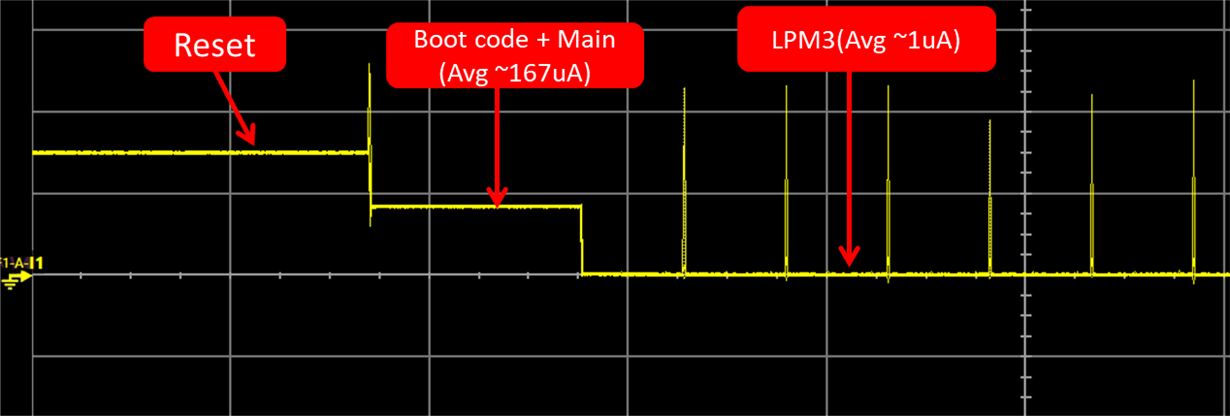
    I put together a code example that accomplishes exactly what you described in your post. I initialize ACLK to run on the low frequency crystal and then configure the ADC capture to trigger the DMA transfer all while not waking up the device or entering into an interrupt. You can find a current consumption screenshot and the code pasted below. From what I can tell, once the boot code executes and we start the ADC samples the device from there on stays in LPM3 current consumption levels (~1uA) except when sampling the ADC and using the DMA for the data transfer (shown as spikes in the current profile).

    #include <msp430.h>
    #include <stdint.h>
    
    int main(void)
    {
      WDTCTL = WDTPW | WDTHOLD;                 // Stop WDT
    
      // Configure GPIOs to it's lowest power state
      P1OUT = 0;                                // All P1.x reset
      P1DIR = 0xFF;                             // All P1.x outputs
      P2OUT = 0;                                // All P2.x reset
      P2DIR = 0xFF;                             // All P2.x outputs
      P3OUT = BIT0;                                // All P3.x reset
      P3DIR = 0xFF;                             // All P3.x outputs
      P4OUT = 0;                                // All P4.x reset
      P4DIR = 0xFF;                             // All P4.x outputs
      PJOUT = 0;                                // All PJ.x reset
      PJDIR = 0xFFFF;                           // All PJ.x outputs
    
      // Set up XT1
      PJSEL0 = BIT4 | BIT5;                     // For XT1
    
      P1SEL0 |= BIT2;                           // configure P1.2/A2 for ADC function
      P1SEL1 |= BIT2;                           //
    
      // Disable the GPIO power-on default high-impedance mode to activate
      // previously configured port settings
      PM5CTL0 &= ~LOCKLPM5;
    
      // Clock System Setup
      CSCTL0_H = CSKEY >> 8;                    // Unlock CS registers
      CSCTL1 = DCOFSEL_0;                       // Set DCO to 1MHz
      CSCTL2 = SELA__LFXTCLK | SELS__DCOCLK | SELM__DCOCLK;
      CSCTL3 = DIVA__1 | DIVS__1 | DIVM__1;     // Set all dividers
      CSCTL4 &= ~LFXTOFF;
    
      do
      {
        CSCTL5 &= ~LFXTOFFG;                    // Clear XT1 fault flag
        SFRIFG1 &= ~OFIFG;
      } while (SFRIFG1 & OFIFG);                // Test oscillator fault flag
    
      // Configure DMA channel 0
      __data20_write_long((uintptr_t) &DMA0SA,(uintptr_t) &ADC12MEM0 );   //Write from ADC12MEM0
                                                // Source block address
      __data20_write_long((uintptr_t) &DMA0DA,(uintptr_t) 0x1C40 );      //Destination address
                                                // Destination single address
      DMACTL0 |= DMA0TSEL_26;                   // DMA triggered by ADC12 End of Conversion
      DMA0SZ = 1;                               // Transfer one byte/word
      DMA0CTL = DMADT_4 | DMAIE; // Rpt single transfer, enable interrupt if GIE is set
      DMA0CTL |= DMAEN;                         // Enable DMA0
    
      ADC12CTL0 = ADC12SHT0_0 | ADC12ON;        // Sampling time, S&H=4, ADC12 on
      // Use TA0.1 to trigger, and repeated-single-channel
      ADC12CTL1 = ADC12SHP | ADC12SHS_1 | ADC12CONSEQ_2;
      // A2 ADC input select; Vref+ = VREF
      ADC12MCTL0 = ADC12INCH_2 | ADC12VRSEL_1 | ADC12EOS;
    
      //ADC12IER0 |= ADC12IE0;                    // Enable ADC interrupt
      ADC12CTL0 |= ADC12ENC | ADC12SC;          // Start sampling/conversion
    
      // Configure Timer0_A3 to periodically trigger the ADC12
      TA0CCR0 = 2048-1;                         // PWM Period
      TA0CCTL1 = OUTMOD_3;                      // TACCR1 set/reset
      TA0CCR1 = 2047;                           // TACCR1 PWM Duty Cycle
      TA0CTL = TASSEL__ACLK | MC__UP;           // ACLK, up mode
    //  __bis_SR_register(LPM3_bits | GIE);       // Enter LPM3, enable interrupts
      __bis_SR_register(LPM3_bits);             //Stay in LPM forever
    
      return 0;
    }

    Best regards,

    Matt

  • Dear Matt,

    Many thanks for your response!

    I've tested your code and it works as expected, but not mine.

    I'm trying to see which is the reason of that, because the codes are very similar.

    Do you believe that the reason could be...

    a) the order in which the peripherals are configured?

    b) the use of __data20_write_long?

    Best and thanks for your time!

    Ferran

  • Ferran,

    As long as the peripherals are configured correctly, and the capture and memory write sequence only starts once the configuring is finished, it should not matter which peripheral is initialized first.

    Also the "data write 16" should be fine since you are not writing to the 20 bit address space.

    I started from separate ADC and DMA code examples and merged them from there to get the example I shared above. In your case, if the example I shared above is working as expected on your hardware then you should be able to work off of that to continue developing your project.

    I am not certain what the differences are between our projects but your best bet is to map out all of the register initializations right before you hit the "__bis_SR_register(LPM3_bits)" line for both projects and see what the differences are from there.

    Best regards,

    Matt

**Attention** This is a public forum