This thread has been locked.

If you have a related question, please click the "Ask a related question" button in the top right corner. The newly created question will be automatically linked to this question.

MSP430F1611: XT2 Drive Strength

Part Number: MSP430F1611

Hi,

Background

An existing design had the XT2 crystal changed to adjust the clock frequency and units began no longer being able to start the crystal. Upon review, the load caps were adjusted slightly to account for trace capacitance which alleviated some of the boards with startup issues, but not all are functioning properly.

Steps Taken

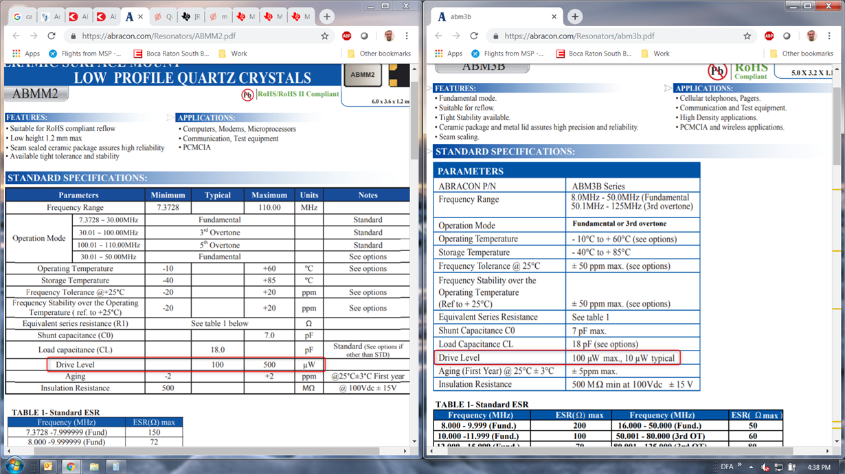
  • Existing crystal ABM3B-8.000MHZ-B2-T was changed to ABMM2-7.3728MHz-E2-T
    • An adjustment of the existing 33pF load capacitors to 27pF capacitors to account for trace capacitance
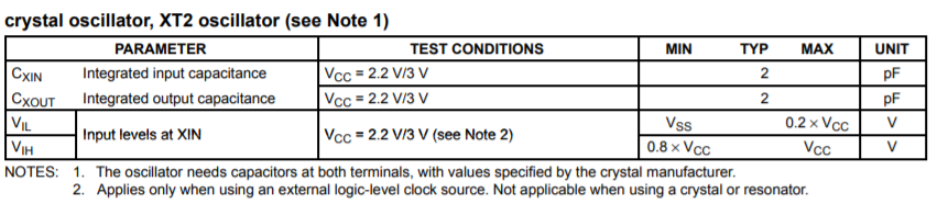
  • Review of the 'F1611 datasheet, XT2 section for drive strength details:
  • Review of the ABM3B and ABMM2 datasheets for crystal differences:

Questions

  1. Is drive strength data of the XT2 peripheral available for the 'F1611 device, or some indication of the maximum supported drive level of a crystal on XT2?
  2. Are any other parameters of the crystal critical to being supported by the 'F1611 device?

Best Regards,

Mark-

  • Hi Mark,
    actually the Drive Level of the crystal is not the parameter to be looked at. This is just defining the limit the crystal is able to cope with. This results from the nature of a crystal, being an electro-mechanical component. Drive levels above the specified value could destroy the crystal, by too large excitation stress.

    Best regards
    Peter
  • The parameter to be looked at in terms of startup and oscillation margin is the ESR. This value is basically reflecting the losses of the crystal, which need to compensated by the oscillator, which is used to drive the crystal, means in our case the XT2.
    The best document to look at for these topics is the application report www.ti.com/.../slaa225a.pdf
    Although mainly addressing 32kHz crystals and oscillators, majority of the aspects and tests described in this application report are applicable also to high frequency crystals.
    When looking at the datasheet screen shots of the two crystals you have provided, the ABM3B-8.000MHZ-B2-T has a 50Ohms higher maximum ESR compared to the ABMM2-7.3728MHz-E2-T. Which means it will probably need a 25% higher drive level from the used oscillator, to compensate the higher losses. This is also indicated by the size of the crystal. While not perfectly linear and comparable across different crystal designs, from tendency point of you one can assume, the smaller the crystal, the higher the losses/ESR, the higher requirements on the used oscillator/driver.
    Looking at the layout you have provided, the XT2 layout is not optimum. There are two main aspects, one is the close by routing of XIN/XOUT, which increases the shunt capacitance between both. This is lowering the performance. The other point is the placement of the load capacitors, which should be placed close to one another, keeping the oscillation signal loop, consisting if the crystal and load capacitors, as small as possible, and the GND electrodes of the load capacitors connected directly as short as possible to one another and to the MSP430 device GND connection.

    To assess the margin of the design with given crystal, the customer would need to perform the safety margin test as described in the application report.
    Another aspect, the XT2 high frequency crystal oscillator is a non regulated oscillator. Its drive level is increasing with the device supply voltage level. Thus if not at 3.6V already, the customer could try to increase the supply voltage.
    Also lowering the load capacitance tends to ease the required drive level conditions with a given crystal (as you noticed), but there is of course a limit, as the load capacitance value is required for accurate frequency, as the nominal frequency is only achieved with specified load capacitance. Too low capacitance makes the crystal oscillate too fast, vice versa too high capacitance slows it down. This is in small ppm range, so potentially not too critical for given application. The more critical aspect are the resulting phase conditions, where at certain minimum load capacitance for given crystal, the setup might become unstable.

    My recommendation would be testing the SFR (see above). If the test results in insufficient margin values, HW change (layout optimization), change of load capacitors, but most probably use of a crystal with lower ESR will be required.

    Best regards
    Peter
  • Hi Mark,
    did my reply answer your/customer's questions? Anything else we could do for you in this case?
    Maybe something to add to put all options on the table.
    The MSP430F2xx family, which contains compatible devices to the MSP430F1611 are equipped with a more modern high frequency crystal oscillator, with adjustable drive levels, with definitely better performance compared to F1xx high frequency oscillator.

    Best regards
    Peter
  • Hi Mark,
    I assume your questions have been answered sufficiently, thus I am closing the thread.

    Best regards
    Peter

**Attention** This is a public forum