This thread has been locked.

If you have a related question, please click the "Ask a related question" button in the top right corner. The newly created question will be automatically linked to this question.

MSP432E401Y: New MSP432 design, start-up problems

Part Number: MSP432E401Y
Other Parts Discussed in Thread: MSP-EXP432E401Y, MSP432E411Y,

I am working on a PCB design using this device, copying all the basic micro-controller circuit from the EXP Eval board schematics.

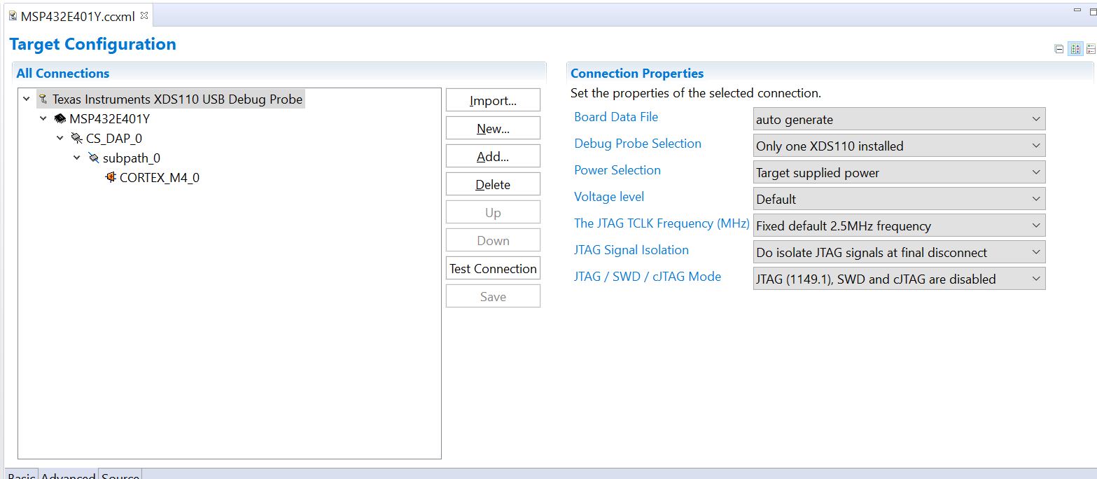
After assembling a first article, we have been unable to communicate with the chip via the JTAG port.

It's very likely that I missed something in copying the reference design, but I can't see it, and need some expert help.

Is there a way to attach a schematic (PDF file), for a start?

Thanks!

Dave

  • Hi,

    Yes, you should be able to do that if you are OK with sharing on the forum.

    see this for help: https://e2e.ti.com/support/site-support/f/1024/t/761613

    regards,

  • I may not have correctly attached the PDF schematic; can't tell from the preview..

    This design is intended to be powered over Ethernet, and the attached schematic is a basic template for several different designs, all using the same processor, power supply, Ethernet with POE, etc.

    Initial software development was done with eval boards (MSP-EXP432E401Y), and the circuit was copied from the published schematics for that board.

    The POE and power regulator circuit was first built and tested by itself, and seemed fine. Vdd was measured at 3.2+ volts, and while it did droop under varying load, it maintained >3.0V up to 250-300mA load. From the MSP432 datasheet, I estimated the absolute maximum current the processor should consume to be well under 200mA.

    Moving on, I added the processor, JTAG connector, Ethernet activity LEDs and what will be an interlock loop output and input. We couldn't get a JTAG debugger probe to complete connection to the MSP or load firmware.

    Vdd was found to be low, at 2.44V, certainly out of spec, so we jumpered in a solid 3.3V from the EXP Eval board we were working with prior to getting our own hardware up. Still no success over JTAG.

    Probing the pins connecting to the two crystals, we see no clocking, which doesn't look good.

    One possible error is that I didn't do anything with the processor's ~Wake input, other than pull it up to Vdd. Momentarily grounding it did nothing, however. That doesn't seem to be used on the Eval board, anyway.

    At this point, I don't know what to look for. Any help and suggestions would be very much appreciated!

    Processor template sch.pdf

  • Thanks for that!  I tried it, hopefully succeeded...

    Dave

  • Just a general comment: There is a System Design Guide for the MSP432E (SLAA770) linked from the Product page. If you haven't been through it yet, maybe it's worth a look. 

    We (believe we) followed all the recommendations in the Guide and our board came up first time.

  • Thank you, Bruce! Yes, we have the design guide, and "We (believe we) followed" it, too.  :{)

    Still digging, but haven't found a smoking gun yet.

  • OK, I just thought I'd mention it. We connected /WAKE (directly) to GND per section 4.15.

    What is the symptom from the JTAG? Sometimes the programmer provides a useful error description.

  • I'll get the latest responses from JTAG when the software guy gets in; I do know there were several different responses, as we fixed minor issues.

    ~Wake is smelling faintly of cordite. I'll get that pin grounded directly, and see what happens.

    Thanks!

  • I looked at the schematics you posted and did not see anything incorrect. 

    Do you have any indication if the MSP432E4 caused the drop in the Vdd from 3.2 to 2.4V? 

    How much is the MSP consuming with the new solid 3.3V provided from the launchpad?  The XDS110 has a limit to the amount of current it will supply. 

    Regards,

    Chris 

  • Thanks for the help, Chris!

    As to whether the MSP432 caused the Vdd drop, I can only say "probably".

    When I first powered it up (via POE), I measured slightly over 3.2V. I passed it to my coworker, who is doing the software and has the Launchpad boards and JTAG tools. After some futzing with connections, he did get some communication with the processor (I'll get details in a little while; Bruce is asking as well), and reported the low Vdd.

    He added a jumper from the Launchpad Vdd, and found a solid 3.3V, but no better operation.

    I'm going to get ~WAKE tied to ground, and see if anything changes. I may possibly be forcing constant interrupts on WAKE ?

  • We didn't experiment with /WAKE -- we just did as we were told (:-)). That might be a red herring. It does sound suspiciously like a power problem.

  • Grounding /WAKE didn't change anything...

    This is what we get from the debugger:

    This error is generated by TI's USCIF driver or utilities.


        The value is '-230' (0xffffff1a).

        The title is 'SC_ERR_PATH_MEASURE'.


        The explanation is:

        The measured lengths of the JTAG IR and DR scan-paths are invalid.

        This indicates that an error exists in the link-delay or scan-path.


    We are using the XDS 110 Debug Probe.  Debug probe works fine when connected to MSP-EXP432E401Y development kit board.

  • Have you attempted to change the frequency of the JTAG connection?  If you are using CCS this is found in the .ccxml file and it you select the 'Advanced' tab you will be able to set the JTAG mode as well as the TCLK frequency.  If there is a mis-match in the trace lengths the lower frequency is a little more forgiving.

    Regards,

    Chris

    EDIT:  Here is link to the specific error and troubleshooting guide: 

  • Thanks, Chris, we will try that.

    I see in the debugger link you sent for the -230 error:

    • If using a XDS510-class debug probe, this means the device configured in the target configuration file (.ccxml) is different than the one attached to the debug probe. This is solved by matching the device chosen in the target configuration editor to the device present in the board

    The device on our assembled board may not be exactly the same as the one on the LaunchPad. Have to experiment with that.

    Due to my error in laying out the JTAG connections on the first board, TMS was swapped with TDO and TCK with TDI.

    This was "fixed" by daisy-chaining two debugger cables end-to-end, with the necessary swaps made by inserting a couple inches of wires between the intermediate sockets.

    Too long over all?

    Poorly matched lengths (but they're quite close to equal)?

  • It is possible that it is too long.  Reducing the clock speed should also help address this. 

    There are only 2 devices in this family, the MSP432E401Y and the MSP432E411Y, which is the BGA package. 

    Regards,

    Chris

  • Tech just finished lifting the JTAG connector ~2cm, making the necessary swaps between the connector and the pcb.

    Now we can run with the single probe cable and no in-line kludges.

    Will get it it into test this afternoon.

  • Hoping no news is good news.  I will close this thread, but feel free to reply or start a new thread using the 'Ask a related question' button.

    Regards,

    Chris

  • Well, still no joy.

    JTAG connector is maybe 1/2" above the PCB, with the correct wires swapped, hooked up to the probe with the correct, single ribbon cable.

    Still complains about "chain length" (or words to that effect.)

    Vdd is at 3.3V, Vddc measured at 1.20V..

    I don't see any JTAG parts in the EXP LaunchPad  schematic except the MSP; am I missing something that's in the probe configuration? Works fine on the LaunchPad, but not on the target board.

    Dave

  • Dave,

    I am going back through the thread.  What was the result to slowing down the JTAG clock?  

    Regards,

    Chris

  • Chris, It's been a few test cycles, but as I recall, no improvement.

    I'm checking with my coworker who is working the test bench, to verify the settings he used and the resulting messages.

    Thanks for following!

    Dave

  • Looks like a great deal of progress today!

    A combination of:

    My PCB layout error (swapping JTAG pins 2 with 6 and 4 with 8), fixed by elevating the connector.

    Non-keyed debug probe connector that was probably inserted backwards for the most recent tests before today.

    We did try lower clock rates, but with the above problems, no joy, obviously....

    Tentatively, this issue is resolved. I'll close the thread by end of day.

    Thanks to all for the help!


    Dave

**Attention** This is a public forum