This thread has been locked.

If you have a related question, please click the "Ask a related question" button in the top right corner. The newly created question will be automatically linked to this question.

MSP430F5529: MSP430F5229, LMX2595

Part Number: MSP430F5529
Other Parts Discussed in Thread: LMX2595, USB2ANY

Respected sir, 

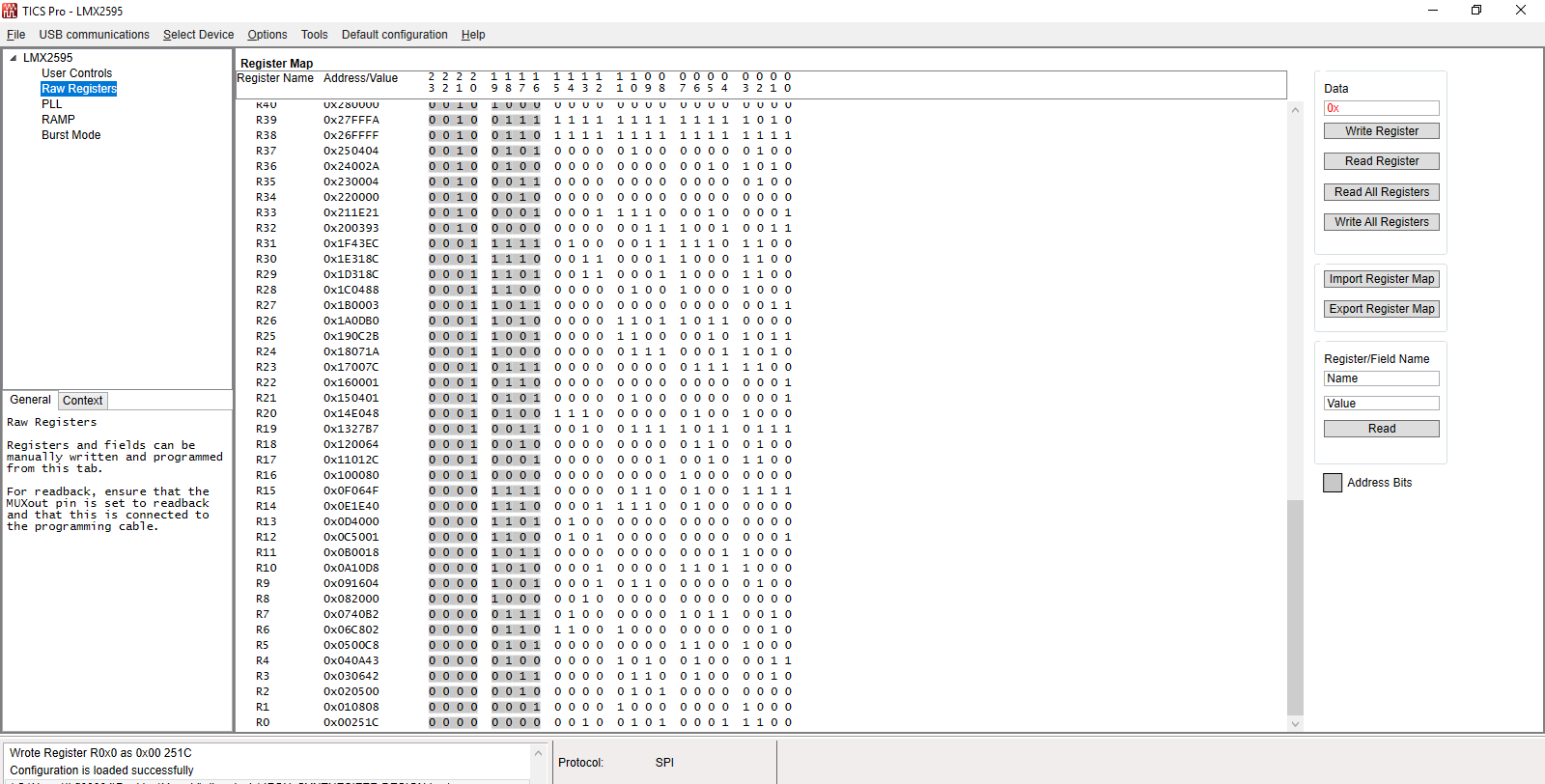
   I am working on LMX2595 and MSP430F5529 to generate 17GHz frequency synthesizer. Now in order to attain this I need to program the micro controller with the values which I get from TICS PRO software. I need to operate the controller in master mode and transfer the data serially to the slave device LMX2595 using SPI protocol. I have came to know that MSP430F5529 has 79x magic constants. Now in order to make use of LMX2595 device as per specific application I need to alter those constants. 

1) How to access those 79x magic constants and alter them by programming?

2) I am not able to find the registers with this memory format as 1-bit R?W, 7-bit Address, 16-bit data in MSP430F5529

3 once the data is transferred to the slave device is it mandatory for the slave device to acknowledge back to the master as the slave device(LMX2595) don't have any MOSI pin.

4) In the programming below control registers of channel 0 has been used, Can I access 79x magic constants and alter the values

Operating MSP430F5529 in Master mode to transfer data 

#include <msp430.h> // header file for msp430 devices
void IOInitiate(void);
void SPI_master_Initiate(void);
void SPI_Tx(char ByteData);
void main(void)
{
WDTCTL=WDTPW+WDTHOLD; // Stop watchdog timer
IOInitiate(); // input output initialization
SPI_master_Initiate(); //master initialization
__bis_SR_register(GIE); // enable interrupts
//return
char sent_to= 'a';

while(1)
{
SPI_Tx(sent_to); // continues sending data

}
}
void IOInitiate(void)
{
P2DIR |= BIT7; // Set P1.0 to output direction for LED
P2OUT &= ~BIT7; //LOW as default
P3SEL |= BIT0+BIT1+BIT2; // P3.0 UCA0SIMO // P3.1 UCA0SOMI // p3.2 clk
P2SEL |= BIT7; // CS
}
void SPI_master_Initiate(void)
{
UCB0CTL1 |= UCSWRST; // **Put state machine in reset**
UCB0CTL0 |= UCMST+UCSYNC+UCCKPL; //8-bit SPI master Clock polarity high, MSB
UCB0CTL0 |= UCMODE_2; // 4 pin communication
UCB0CTL1 |= UCSSEL_2; // SMCLK // clock selection

UCB0BR0 = 0x00; // SMCLK speed divide by 1 /*******If UCBRx = 0, fBitClock = fBRCLK****/
UCB0BR1 = 0;
UCA0MCTL = 0; // No modulation
UCB0CTL1 &= ~UCSWRST; // **Initialize USCI state machine**
UCB0IE |= UCTXIE; // receving interrupt enable
}
void SPI_Tx(char ByteData)
{
P2OUT &= ~BIT7; // active low for start communication

UCB0TXBUF = ByteData; // Transmit first character

//if (UCB0TXBUF!=ByteData)

while (!(UCB0IFG&UCTXIFG)) ; //hold until transmit finish

P2OUT |= BIT7; // active High for end communication

}

I am a newbie and running out of time. Any help will be greatly appreciated. 

Thanks in Advance.

  • The 79x "magic" constants are those register values you see on the TICS Pro screen (R78, R77, etc). (I think) you want to capture those values and insert them into your F5529 program as an array.

    I see an "Export" button over to the right, which I suspect will create a text file (in some format) containing the values on the screen. You should edit the "0X" constants so they look somewhat like:

    unsigned long register_values[79] = {  // LMX2595 register values with SPI prefix
      0x4E0003, // R78
      0x4D0000, // R77
      0x4C000C, // R76
    [...]
    }; // end of register_values[]

    then in your program have something like:

    void write_register(unsigned long value) {
      SPI_Tx((value >> 16) & 0xFF);  // Register number+R/W
      SPI_Tx((value >>  8) & 0xFF);   // Register value high byte
      SPI_Tx((value >>  0) & 0xFF);   //  Register value low byte
    }

    then in main

      for (reg = 0 ; reg < 79 ; ++reg) write_register(register_values[reg]);

    I've probably got some details wrong (since I don't have any of this equipment), but I think this is the general idea.

  • Sir, I have implemented as per the above changes but still I am facing some difficulties. At present I don't have launch pad kit and I faced an error which is due to the hardware pin I have defined. I have transferred the data which I have loaded into an array size of 79. I don't think that the memory space which has been created has the register map starting with the 1-bit r/w, 7-bit address, 16-bit data. 

    I am attaching the code below, kindly let me know the necessary changes

    #include <msp430.h>
    unsigned long register_values[79]
    void SPI_Tx(value bytedata)
    void IOInitiate(void);
    void SPI_master_Initiate(void);
    void write_register(unsigned long value)
    {
    SPI_Tx((value>>16) & 0xFF);
    SPI_Tx((value>>8) & 0xFF);
    SPI_Tx((value>>0) & 0xFF);
    }

    /**
    * main.c
    */
    int main(void)
    {
    WDTCTL = WDTPW | WDTHOLD; // stop watchdog timer
    IOInitiate(); // input output initialization
    SPI_master_Initiate(); //master initialization
    __bis_SR_register(GIE); // enable interrupts
    return 0;
    }
    void write_register(unsigned long value)
    unsigned long register_values[79] = {0x00251C,0x010808,0x020500,0x030642,0x040A43,0x0500C8,0x06C802,0x0740B2,0x082000,0x091604,0x0A10D8,0x0B0018,0x0C5001,0x0D4000,0x0E1E40,0x0F064F,0x100080,0x11012C,0x120064,0x1327B7,0x14E048,0x150401,0x160001,0x17007C,0x18071A,0x190C2B,0x1A0DB0,0x1B0003,0x1C0488,0x1D318C,0x1E318C,0x1F43EC,0x200393,0x211E21,0x220000,0x230004,0x24002A,0x250404,0x26FFFF,0x27FFFA,0x280000,0x290000,0x2A7FFF,0x2BFFFD,0x2C0AE3,0x2DD0DF,0x2E07FD,0x2F0300,0x300300,0x314180,0x320000,0x330080,0x340820,0x350000,0x360000,0x370000,0x380000,0x390020,0x3A8001,0x3B0001,0x3C0000,0x3D00A8,0x3E0322,0x3F0000,0x401388,0x410000,0x4201F4,0x430000,0x4403E8,0x450000,0x46C350,0x470081,0x480001,0x49003F,0x4A0000,0x4B0800,0x4C000C,0x4D0000,0x4E0003}

    void IOInitiate(void)
    {
    P2DIR |= BIT7; // Set P2.0 to output
    P2OUT &= ~BIT7; //LOW as default
    P3SEL |= BIT0+BIT2; // P3.0 UCA0SIMO // p3.2 clk
    P2SEL |= BIT7; // CS
    }
    void SPI_master_Initiate(void)
    {
    UCB0CTL1 |= UCSWRST; // **Put state machine in reset**
    UCB0CTL0 |= UCMST+UCSYNC+UCCKPL; //8-bit SPI master Clock polarity high, MSB
    UCB0CTL0 |= UCMODE_2; // 4 pin communication
    UCB0CTL1 |= UCSSEL_2; // SMCLK // clock selection
    UCB0BR0 = 0x00; // SMCLK speed divide by 1 /*******If UCBRx = 0, fBitClock = fBRCLK****/
    UCB0BR1 = 0;

    UCA0MCTL = 0; // No modulation
    UCB0CTL1 &= ~UCSWRST; // **Initialize USCI state machine**
    UCB0IE |= UCTXIE; // receving interrupt enable
    }

    for(reg=0; reg<79; reg++)
    {
    write_register(register_values[reg])
    }

    Thanks in advance


  • What error are you facing? This code as posted won't compile (the for() loop is not in main(), there are some missing semicolons) but maybe those are just copy/paste errors. When I fixed those up, the register_value[] array looked correct in a Listing file.

    Also, if you don't have a Launchpad, where is your F5529 chip? I haven't found one on the EVM; the EVM Guide suggests there might be one on the USB2ANY but (when I looked a few weeks ago) I didn't find any schematics for that board, so I don't know. (I'll just mention here that the F5529 Launchpad is $13US at the TI Store, and it does have published schematics.)

    More generally: What do you hope to have when you're finished? Do you plan to keep using the EVM (probably fine for a laboratory environment) or will you be building a custom board to be deployed in some product? 

    ------------------------------

    Specifics: 

    > P2SEL |= BIT7; // CS

    > UCB0CTL0 |= UCMODE_2; // 4 pin communication

    I think you want 3-wire (with /CS as a GPIO), i.e. UCMODE_0 and don't set P2SEL.7, since you need to hold /CS low over multiple bytes.

    ---

    > UCB0IE |= UCTXIE; // receving interrupt enable

    Remove this line. You don't have anything set up for SPI interrupts, and you don't want to use them anyway.

    ---

    Here is a function I keep finding myself writing. It's mostly like your (earlier) SPI_Tx() but (a) you can freely mix transmit-only and transmit+receive transactions (b) it's always safe to de-assert /CS (c) it's faster (for a fast SPI such as yours) than interrupts.

    uint8_t spix(uint8_t c)
    {
      while (!(UCB0IFG & UCTXIFG)) /*EMPTY*/;
      UCB0TXBUF = c;
      while (!(UCB0IFG & UCRXIFG)) /*EMPTY*/;
      c = UCB0RXBUF;
      return(c);
    }

  • Actually I need to dump the code in the MSP430F55229 and later on need to fabricate it on the pcb board in the project which of frequency synthesizer. I have placed the order for launchpad kit, where in I am going to test the code. 

    1) At present I am facing FATAL error which I think it is due to the function SPI_Tx which I thought it is builtin function.

    I am hereby attaching the code below, Kindly let me know the changes required sir. As far as my knowledge I am upto this level and I am newbie sir kindly look into it sir

    #include <msp430.h>

    #include <stdint.h>

    #include <stdbool.h>

    unsigned long register_values[79]

    //void SPI_Tx(register_values[79])

    //void IOInitiate(void);

    //void SPI_master_Initiate(void)


    int main(void)

    {

       WDTCTL = WDTPW | WDTHOLD; // stop watchdog timer

       IOInitiate(); // input output initialization

       SPI_master_Initiate(); //master initialization

       //__bis_SR_register(GIE); // enable interrupts

       return 0;


    unsigned long register_values[79] = {0x00251C,0x010808,0x020500,0x030642,0x040A43,0x0500C8,0x06C802,0x0740B2,0x082000,0x091604,0x0A10D8,

                                         0x0B0018,0x0C5001,0x0D4000,0x0E1E40,0x0F064F,0x100080,0x11012C,0x120064,0x1327B7,0x14E048,0x150401,

                                        0x160001,0x17007C,0x18071A,0x190C2B,0x1A0DB0,0x1B0003,0x1C0488,0x1D318C,0x1E318C,0x1F43EC,0x200393,

                                         0x211E21,0x220000,0x230004,0x24002A,0x250404,0x26FFFF,0x27FFFA,0x280000,0x290000,0x2A7FFF,0x2BFFFD,0x2C0AE3,

                                         0x2DD0DF,0x2E07FD,0x2F0300,0x300300,0x314180,0x320000,0x330080,0x340820,0x350000,0x360000,0x370000,0x380000,

                                         0x390020,0x3A8001,0x3B0001,0x3C0000,0x3D00A8,0x3E0322,0x3F0000,0x401388,0x410000,0x4201F4,0x430000,0x4403E8,

                                         0x450000,0x46C350,0x470081,0x480001,0x49003F,0x4A0000,0x4B0800,0x4C000C,0x4D0000,0x4E0003};


    unsigned long int reg;

    for(reg=0; reg<79; reg++)

       {

       write_register(register_values[reg]);


           void write_register(register_values[79]);


               void SPI_Tx(char register_values[reg])

               {

               SPI_Tx((char register_values[reg]>>0) & 0xFF); // To transfer data serially bit by bit and right shifted 

               SPI_Tx((char register_values[reg]>>8) & 0xFF);

               SPI_Tx((char register_values[reg]>>16) & 0xFF);

               }


       }


    uint8_t spix(uint8_t c)

    {

       while(!(UCB0IFG & UCTXIFG))

           UCTXIFG = c;

       while (!(UCB0IFG & UCRXIFG))

           c = UCRXIFG;

       return(c);

    }

    }


    void IOInitiate(void)

    {

    P2DIR |= BIT7; // Set P2.0 to output

    P2OUT &= ~BIT7; //LOW as default

    P3SEL |= BIT0+BIT2; // P3.0 UCA0SIMO // p3.2 clk

    P2SEL |= BIT7; // CS

    }

    void SPI_master_Initiate(void)

    {

    UCB0CTL1 |= UCSWRST; // **Put state machine in reset**

    UCB0CTL0 |= UCMST+UCSYNC+UCCKPL+UCMSB; //8-bit SPI master Clock polarity high, MSB

    UCB0CTL0 |= UCMODE_2; // 4 pin communication

    UCB0CTL1 |= UCSSEL_2; // SMCLK // clock selection

    UCB0BR0 = 0x00; // SMCLK speed divide by 1 /*******If UCBRx = 0, fBitClock = fBRCLK****/

    UCB0BR1 = 0;


    UCA0MCTL = 0; // No modulation

    UCB0CTL1 &= ~UCSWRST; // **Initialize USCI state machine**

    //UCB0IE |= UCTXIE; // receving interrupt enable

    }


    Any help will be greatly appreciated sir,

    Thanks in advance,

    Regards

    singam vamshi.

  • 1) I offered spix() as a replacement for your (earlier) SPI_Tx function. You can change the name to SPI_Tx if you like.

    2) You should go back and re-copy the spix() source I posted above, since this one has been modified such that it won't work.

    3) I don't recommend using UCMODE_2, since that won't allow you multi-byte transactions. From your code, you appear to have connected /CS to P2.7. I recommend (a) use UCMODE_0 (b) remove the line "P2SEL |= BIT7; " (c) in write_register, add "P2OUT &= ~BIT7;" at the beginning and "P2OUT |= BIT7;" at the end; this will lower /CS before the transaction and raise /CS at the end.

    With that, I think you have the pieces you need, you just need to edit them into a valid C program.

    [Edit: Fixed typo.]

**Attention** This is a public forum