This thread has been locked.

If you have a related question, please click the "Ask a related question" button in the top right corner. The newly created question will be automatically linked to this question.

MSP430I2021: Questions about external resistor tolerance and calibration, different clock frequency and unique memory identifiers

Expert 6310 points
Part Number: MSP430I2021
Other Parts Discussed in Thread: MSP430F148

Team,

we are prototyping with I2021 and have a few questions,

We will use external resistor for the oscillator. The tolerance of the resistor recommended in the datasheet is 0.1%, but in practice it's possible we'll have a resistor with slightly different value / a bit worse tolerance. As a consequence we will need to calibrate the frequency and memorize the CSERFCAL register value.

  1. What is the meaning of each register bits? Alternatively, how to calibrate the frequency (by +/- few percent range)?
    1. We assume we can measure the MLCK frequency (directly or its subdivision) and change the value in CSREFCAL through serial interface.
  2. From different reasons we would prefer to use 16MHz instead of 16,384MHz clock. This yields the clock of the a/d converter of 1MHz, instead of the recommended 1.024MHz.
    1. Can it impact negatively and visibly the operation of the converter and of the whole device?
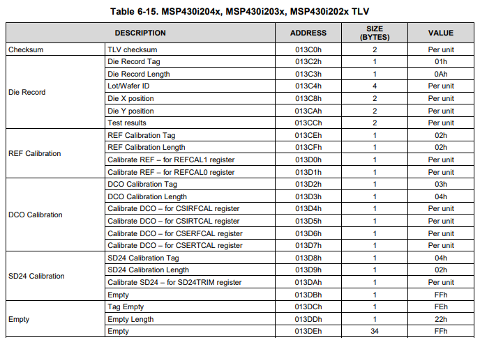
  3. Do MSP430i20xx have in their primary memory any identifiers that would help to identify them? If so, where/how?
    1. For example, MSP430F148 has 0xf149 under 0x0ff0 address.

Thank you.

  • Hi Bart,

    Bart said:
    we are prototyping with I2021 and have a few questions,

    Thanks so much for your post. Prototyping is fun!

    Bart said:

    We will use external resistor for the oscillator. The tolerance of the resistor recommended in the datasheet is 0.1%, but in practice it's possible we'll have a resistor with slightly different value / a bit worse tolerance. As a consequence we will need to calibrate the frequency and memorize the CSERFCAL register value

    You're correct. Table 5-2 in the datasheet recommends using a 20 kΩ, 0.1%, ±50 ppm/°C resistor for ROSC in External Resistor Mode.

    Bart said:
    What is the meaning of each register bits? Alternatively, how to calibrate the frequency (by +/- few percent range)?

    1. We assume we can measure the MLCK frequency (directly or its subdivision) and change the value in CSREFCAL through serial interface.

    In External Resistor Mode, I would start with the calibrated CSERFCAL and CSERTCAL register values and the desired 20kΩ resistor. Check the accuracy. Before doing anything though, I would back up the entire INFO memory for each device since these default calibration factors are device-specific and are easily erasable during debug and programming.

    Unfortunately, I'm not sure what each bit in the CSERFCAL and CSERFCAL registers impacts. Table 6-18 in the datasheet just says they are "clock system external resistor frequency calibration" and "clock system external resistor temperature calibration" registers, respectively.

    I do like your idea of backing up the original values and changing them while measuring the MCLK output. I would start at the original value and increment up/down bit-by-bit. The frequency should be close with the original values, so hopefully you wouldn't need to change them much.

    When making these changes, I would recommend following the Application Use Cases in Section 4.2.4 in the user's guide.

    Bart said:
    From different reasons we would prefer to use 16MHz instead of 16,384MHz clock. This yields the clock of the a/d converter of 1MHz, instead of the recommended 1.024MHz.

    2. Can it impact negatively and visibly the operation of the converter and of the whole device?

    Yes, each module may have a different maximum input clock specification, but the CPU can definitely operate at 16 MHz. See the specification of the respective module in this data sheet. Section 4.2.2 in the user's guide says "If SD24 functionality is desired in DCO bypass mode, an 16.384-MHz clock should be provided at the CLKIN pin. The SD24 module does not operate reliably if the external clock frequency in bypass mode is not 16.384 MHz." and Footnote 1 under Table 5-5 in the datasheet says "External digital clock frequency in DCO bypass mode must be 16.384 MHz for the SD24 module to meet the specified performance.". Thus, the same would apply for when the internal DCO is not operating at 16.384 MHz. To me, it sounds like the SD24 ADC performance would suffer, but I can't say what metric or if all of them would degrade. I'd say test it and see if the accuracy still meets your requirements.

    Bart said:
    Do MSP430i20xx have in their primary memory any identifiers that would help to identify them? If so, where/how?

    3. For example, MSP430F148 has 0xf149 under 0x0ff0 address.

    That's an interesting question. I don't think that's documented anywhere. However, there may be some unique value in the TLV that you could use to identify this device family. Perhaps you could use the 0xFE22 at 0x13DC to 0x13DD. I couldn't find the TLV info in the MSP430F148 datasheet to compare.

    Regards,

    James

  • Hi James,

    thanks for your feedback, appreciate. We would, however, need some more detailed answers regarding questions 1. and 2. - are you able to provide an example code which could be used to calibrate the device accordingly? From the user guide and datasheet references that you shared, it is not clear how to perform the calibration step by step. An example code and/or some step by step guide would be very, very helpful.

    Also, if the 16MHz clock is used, do we know if there will be any (harmful) effect of this in the longterm operation of the device? Or is it fine?

    Thank you.

    Kind regards,

    Bart

  • Hi Bart,

    Unfortunately, I am not able to provide any additional feedback or a code example on how to do this. The MSP430i20xx was intended to run at a fixed DCO frequency, so there's no resources available that describe adjusting the DCO frequency. You can take advantage of the bypass feature that allows an external clock signal to be used instead.

    Regarding effects on the ADC, the way the datasheet reads seems to indicate that the ADC performance (e.g. accuracy, noise rejection, etc.) won't be as specified in the datasheet. That doesn't sound like long term damage to me, but we do recommend a 16.384 MHz clock be used to provide a 1.024 MHz signal to the ADC.

    Regards,

    James

**Attention** This is a public forum