This thread has been locked.

If you have a related question, please click the "Ask a related question" button in the top right corner. The newly created question will be automatically linked to this question.

MSP430FR2676: Can't get I2C Peripheral to work - have to be missing something so simple!!

Part Number: MSP430FR2676
Other Parts Discussed in Thread: CAPTIVATE-FR2676, CAPTIVATE-PGMR, , MSP430FR2476

Good Morning,

 I have to be missing something so simple!  I know will feel dumb when someone shows me what I missed - but at this point - I can take it!!

  • Any help will be so much appreciated :)

 QUESTION:

  • What dumb setting am I missing?

SYMPTOM:

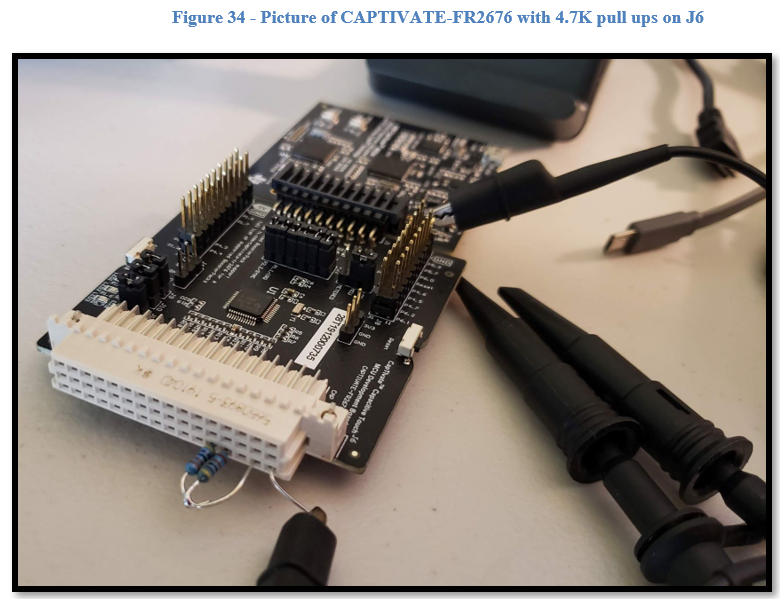
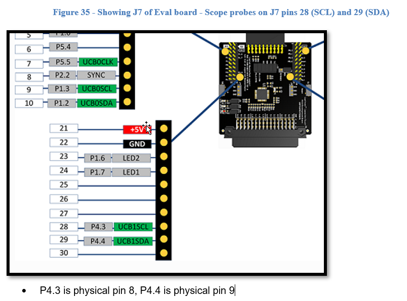
  • Have scope on P4.3 (SCL) & P4.4 (SDA) of CAPTIVATE-FR2676 Eval board (J7 pins 28 & 29)- and NEVER see any activity (yes my scope is set up correctly LOL)

 INFO:

  • I am using CCS, with the CAPTIVATE-PGMR & CAPTIVATE-FR2676 Eval board (MSP430FR2676TPTmicro - 48 LQFP package).
    • No Slave is attached but configuring as Master so should still see something
    • Have external 4.7K ohm pull ups on SCL and SDA


  • I used Example code MSP430FR267x_euscib0_i2C_15 as starting point: (Master Code)
    • Again want as master – so can see sending out Slave Address
    • The example uses euscib0.
    • Changed code to uses euscib1 (so exposed on J7 header of Eval board – can scope)
    • Changed PxSEL registers to use P4.3 (CLK) and P4.4 (SDA) so again can scope.
    • Those were the only changes made!!


  • I did NOT try the Example code right out of box – since believe the Programmer board is using to program the MSP430.

 Again – can’t thank you enough – pull what little hair left on my head out!!

 Willie

 ----------------------------

 --------------------

Actual Code:

//  MSP430FR267x Demo - eUSCI_B0 I2C Master TX bytes to Multiple Slaves
//
//  Description: This demo connects two MSP430's via the I2C bus.
//  The master transmits to 4 different I2C slave addresses 0x0A,0x0B,0x0C&0x0D.
//  Each slave address has a specific related data in the array TXData[].
//  At the end of four I2C transactions the slave address rolls over and begins
//  again at 0x0A.
//  ACLK = REFO = 32768Hz, MCLK = SMCLK = default DCO = ~1MHz
//  Use with msp430fr267x_eUSCIB_04.c
//
//                                /|\  /|\
//               MSP430FR2676      10k  10k     MSP430FR2676
//                   slave         |    |        master
//             -----------------   |    |   -----------------
//            |     P1.2/UCB0SDA|<-|----|->|P1.2/UCB0SDA     |
//            |                 |  |       |                 |
//            |                 |  |       |                 |
//            |     P1.3/UCB0SCL|<-|------>|P1.3/UCB0SCL     |
//            |                 |          |             P1.0|--> LED
//
//   Longyu Fang
//   Texas Instruments Inc.
//   August 2018
//   Built with IAR Embedded Workbench v7.12.1 & Code Composer Studio v8.1.0
//******************************************************************************
#include <msp430.h>

unsigned char TXData[]= {0xA1,0xB1,0xC1,0xD1};        // Pointer to TX data
unsigned char SlaveAddress[]= {0x0A,0x0B,0x0C,0x0D};
unsigned char TXByteCtr;
unsigned char SlaveFlag = 0;

int main(void)
{
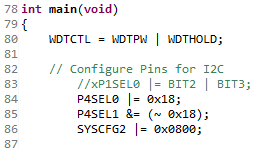
    WDTCTL = WDTPW | WDTHOLD;                         // Stop watchdog timer

    // Configure Pins for I2C
        //xP1SEL0 |= BIT2 | BIT3;                       // I2C pins
        P4SEL0 |= 0x18;                                 // configure I2C pins (device specific)
        P4SEL1 &= (~ 0x18);                             //Using Physical pins 8,9 of MSP430FR2676TPT (48 LQFP package on Captivate MSP430FR2676 Eval board)

    // Disable the GPIO power-on default high-impedance mode
    // to activate previously configured port settings
    PM5CTL0 &= ~LOCKLPM5;

    // Configure USCI_B0 for I2C Master Mode
    UCB1CTLW0 |= UCSWRST;                             // put eUSCI_B in reset state
    UCB1CTLW0 |= UCMODE_3 | UCMST | UCSYNC;           // I2C master mode, SMCLK, UCA10 = 0 by default from reset
    UCB1BRW = 0x8;                                    // baudrate = SMCLK / 8
    UCB1CTLW0 &=~ UCSWRST;                            // clear reset register
    UCB1IE |= UCTXIE0 | UCNACKIE;                     // transmit and NACK interrupt enable

    SlaveFlag =0;

    while(1)
    {
    __delay_cycles(1000);                             // Delay between transmissions
    UCB1I2CSA = SlaveAddress[SlaveFlag];              // configure slave address
    TXByteCtr = 1;                                    // Load TX byte counter
    while (UCB1CTLW0 & UCTXSTP);                      // Ensure stop condition got sent
    UCB1CTLW0 |= UCTR | UCTXSTT;                      // I2C TX, start condition
                                                            //(***** Expect to see some I2C clock signals on scope - but DON'T :(  )

   // __bis_SR_register(LPM0_bits | GIE);               // Enter LPM0 w/ interrupts
                                                      // Remain in LPM0 until all data
                                                      // is TX'd

    // Change Slave address
    SlaveFlag++;
    if (SlaveFlag>3)                                  // Roll over slave address
      {
        SlaveFlag =0;
      }
    }

}


#pragma vector = EUSCI_B1_VECTOR
__interrupt void USCI_B1_ISR(void)
{
  switch(__even_in_range(UCB1IV,USCI_I2C_UCBIT9IFG))
  {
        case USCI_NONE: break;                        // Vector 0: No interrupts break;
        case USCI_I2C_UCALIFG: break;
        case USCI_I2C_UCNACKIFG:
            UCB1CTL1 |= UCTXSTT;                      //resend start if NACK
          break;                                      // Vector 4: NACKIFG break;
        case USCI_I2C_UCSTTIFG: break;                // Vector 6: STTIFG break;
        case USCI_I2C_UCSTPIFG: break;                // Vector 8: STPIFG break;
        case USCI_I2C_UCRXIFG3: break;                // Vector 10: RXIFG3 break;
        case USCI_I2C_UCTXIFG3: break;                // Vector 14: TXIFG3 break;
        case USCI_I2C_UCRXIFG2: break;                // Vector 16: RXIFG2 break;
        case USCI_I2C_UCTXIFG2: break;                // Vector 18: TXIFG2 break;
        case USCI_I2C_UCRXIFG1: break;                // Vector 20: RXIFG1 break;
        case USCI_I2C_UCTXIFG1: break;                // Vector 22: TXIFG1 break;
        case USCI_I2C_UCRXIFG0: break;                // Vector 24: RXIFG0 break;
        case USCI_I2C_UCTXIFG0:
        if (TXByteCtr)                                // Check TX byte counter
           {
            UCB1TXBUF = TXData[SlaveFlag];            // Load TX buffer
            TXByteCtr--;                              // Decrement TX byte counter
           }
        else
           {
            UCB1CTLW0 |= UCTXSTP;                     // I2C stop condition
            UCB1IFG &= ~UCTXIFG;                      // Clear USCI_B0 TX int flag
            __bic_SR_register_on_exit(LPM0_bits);     // Exit LPM0
           }
          break;                                      // Vector 26: TXIFG0 break;
        case USCI_I2C_UCBCNTIFG: break;               // Vector 28: BCNTIFG
        case USCI_I2C_UCCLTOIFG: break;               // Vector 30: clock low timeout
        case USCI_I2C_UCBIT9IFG: break;               // Vector 32: 9th bit
        default: break;
  }


}

  • Try adding [Ref UG (SLAU445I) Table 1-26, DS (SLASEO5A) Table 4-2]:

    > SYSCFG2 |= USCIBRMP;  // Use P4, not P3, for UCBx

  • Hi Bruce!!

    Thank you so much for such a quick reply :)

    • I think you got me 100% on the right track but still might be missing something (don't see any SCLK on scope on pin  P4.3)
    • I am sure that SYSCFG2 is part of my issue and I added .

    QUESTION:

    • Do I have to add at a certain point in the code?
    • Could it be since using the CAPTIVATE_PGMR - is already using eUSCIB0 - and messing me up?
    • If so - can I change that somehow in project settings or?

    Again - thank you so much - (you are saving what little hair I have left!!)

    Willie

    -------------------------

    Snippit of where added SYSCFG2 setting - right toward beginning of main

  • Setting the USCIBRMP switches both UCB1 and UCB0 to the alternate pin-pairs, but I expect that by that time the PGMR is already out of the way.

    Since you removed the line that enables interrupts (GIE) you would only get one shot at capturing the first (SLA) byte. In that case, though, I would expect to see SCL held low (forever) since the I2C is stretching the clock, waiting for you to respond to the TXIFG.

  • Hi again Bruce,

    Thank you again for you patience with me:

    • No Mater what I have tried - I NEVER have seen a single CLK cycle on P4.3 :(

    Is there anything else I can be missing?

    Thank you

    Willie

    ---------------------

    I was tired of looking at straight lines on my scope LOL - so I did a quick Level Set:

    • I used the EXACT code in example code MSP430FR267x_euscib0_i2c_15 (master code)
    • On the MSP430FR2676 Eval board (it does expose P1.2 & P1.3 on the stickheader J7) - put scope probes on these signals
    • These are the pins used by the default eUSCIB0 for I2C
    • Low and behold - I see goodness (clocks and data everywhere YEAH!)

    BUT - for the life of me can't see this on P4.3 & P4.4 even when change the SYSCFG2 to set USCIBRMP = 1

    • I am honestly stuck.  No idea what else to even try
    • I even looked at the errata sheet and couldn't find anything
    • I'm sure not the FIRST person to try this LOL 

  • Hi Willie,

    I think there is something wrong with the re-mapping.

    According to the UG SLAU445I Table 1-32 the USCIB1RMP is defined in the SYSCFG3 register.

    Can you try that out.

    Regards

    Kostas

  • Good Morning Kostas!

    Oh My Gosh!!  You did it - you fixed me!!  Can I buy you and Bruce a beer - how about a CASE of BEER!!

    • I am up and running!!  Whew - 2 days of going crazy!!

    INFO:

    • Kostas - you are correct - USCIB1RMP is NOT located in SYSCFG2
    • USC1B1RMP (for remapping to alternate pin out) is located in SYSCFG3 (bit 4) - just as you mentioned above!!
    • I will mark this as resolved!!!

    Thank you both so much for your support (you both ROCK!!)

    Willie

  • Thanks for finding this.

    Curious that SLASEO5A specifically mentions USCIBRMP (in SYSCFG2) multiple times, and doesn't mention USCIB1RMP at all. [Ref DS (SLASEO5A) Sec 6.10.7, Table 6-11 Note (1)-(2), Table 4-2 Note (3)-(4)], 

    [Edit: Rev C says the same thing.]

    [More Edit: The MSP430FR2476 data sheet (SLASEO7B) reads the same way. It also has UCB1 and no SAC, and doesn't mention USCIB1RMP, only USCIBRMP. I actually have one of these. Is it useful for me to try this?]

  • Hi Bruce,

    you are right it's not very clear. There may be an "x" missing indicating the different modules.

    It's in the UG (SLAU445I) Table 1-32.

    Regards

    Kostas

  • I respectfully suggest that the data sheet (which is authoritative) is clear, it's just incorrect.

    I've submitted a document-error report for SLASEO7B, and I included a suggestion that SLASEO5C may have the same mistake (I don't have an FR2676 to work with).

  • Thanks Bruce for filing the error report.

    Regards

    Kostas

**Attention** This is a public forum