Hello everyone,
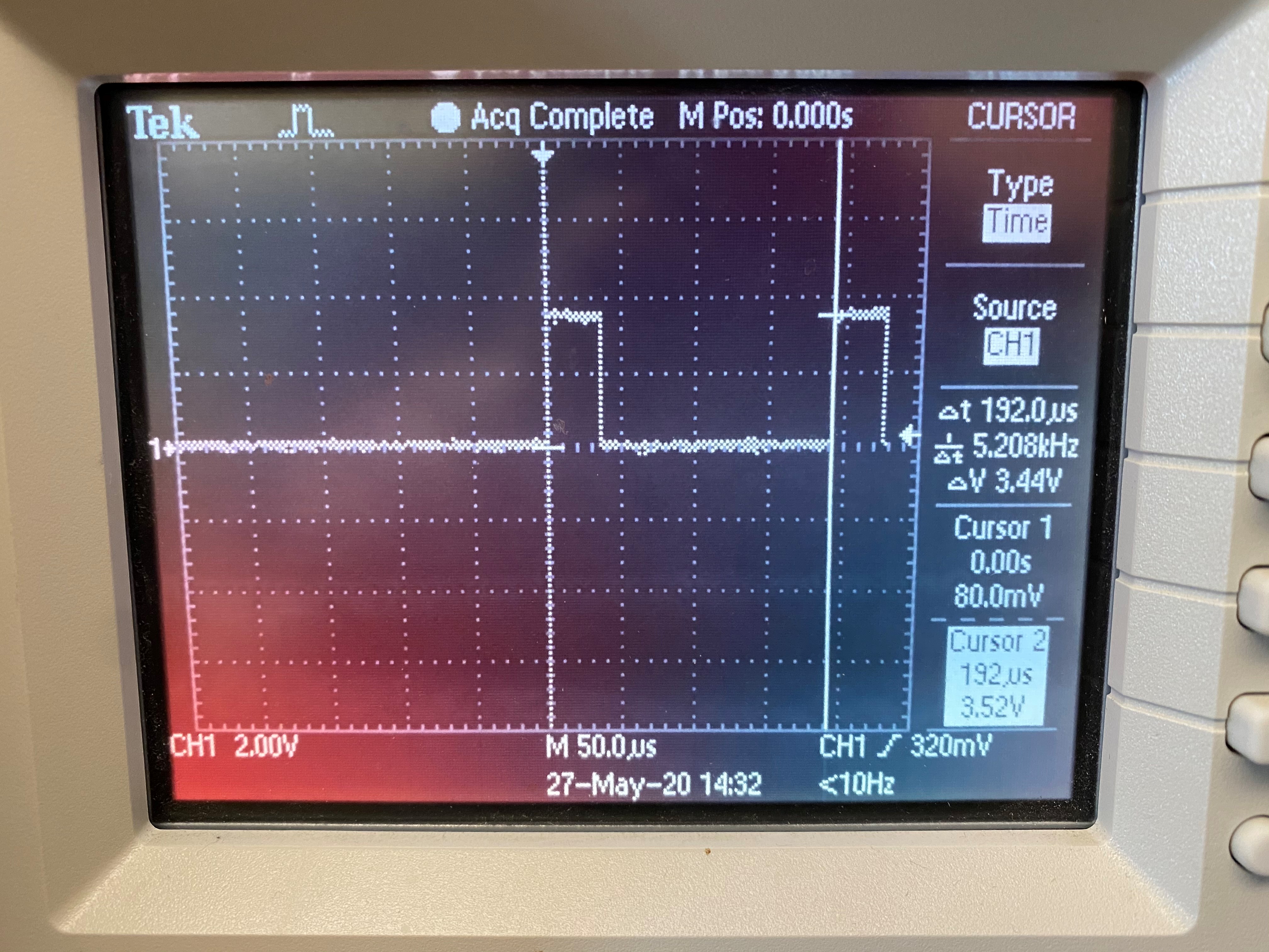
I am new to the MSP430 platform and I working on a project where a double pulse needs to generated with a 200us delay between both rising edges (see picture attached). I am currently trying to use Timer B to generate these signals. currently using standard 1MHz SMCLK for input to timer B.
The code below is what I currently have and I am not understanding how the TBxCCRn register are working. I was wondering if someone could help out? or provide a better explanation that the one that is the datasheet / family user manual? What is confusing me is the values that are being placed into the TB1CCR1 and TB1CCR2 registers
Thank you for all the help in advance.
#include <msp430.h>

int main(void)
{
    WDTCTL = WDTPW | WDTHOLD;  //stops the watchdog timer.


    //Trigger Input (P1.0)
    P1DIR &= ~BIT0;
    P1REN |= BIT0; //enable internal pullup/pulldown resistors
    P1OUT |= BIT0; // select pull-up mode for P1.0
    P1IE |= BIT0; //enable interrupts
    P1IES |= BIT0; //high -> low sets flag
    P1IFG &= ~BIT0; //interrupt flag register cleared


    //output on p1.1 (INIT_Q_DRIVE)
    P1DIR |= BIT1; // setting direction on specific pin
    P1OUT &= ~BIT1; // setting the initial output to 0


    PM5CTL0 &= ~LOCKLPM5; //disable GPIO power-on default to activate previously configured settings

    //TB1CCTL1 |= (OUTMOD_7 | CCIE); // Timer B1 Capture/Compare Control Register1 is set to Set/Reset
    TB1CCTL1 |= CCIE; //Timer B1 Capture/Compare Control Register1 enabled for interrupts

    //TB1CCTL2 |= (OUTMOD_7 | CCIE); // Timer B1 Capture/Compare Control Register1 is set to Set/Reset
    TB1CCTL2 |= CCIE; //Timer B1 Capture/Compare Control Register1 enabled for interrupts

    TB1CCR1 = 10;
    TB1CCR2 = 20;

    while(1){
        __bis_SR_register(LPM3_bits | GIE); //enter low power mode and enable interrupts
    }
}

// interrupt on I/O port (pin P1.0)
#pragma vector = PORT1_VECTOR
__interrupt void Port_1_ISR(void)
{

    P1IE &= ~BIT0; //disable interrupts so none occur while in this routine
    P1IFG &= ~BIT0; //clear interrupt flag that occured on p1.0

    //below the different delay times need to be set (200, 400, 800, 1000 us)
    //check input pins to see what has been selected. checked based on rotary switch

    TB1CCR0 = 208; //200us delay (this hardcoding is temporary)

    //start timer
    TB1CTL = TBSSEL_2 | MC_1 | TBCLR | TBIE; // Starting the timer, SMCLK(1MHz), UP mode, clear TBR, enable interrupt
}

//timer b interrupt service routine when timer b causes an interrupt this is called
#pragma vector = TIMER1_B1_VECTOR
__interrupt void TIMER1_B1_ISR(void)
{
     switch(__even_in_range(TB1IV,TB1IV_TBIFG))
    {
        case TB1IV_NONE:
            break; // No interrupt

        case TB1IV_TBCCR1:
            P1OUT ^= BIT1; //Output...rising edge of both waves
            break;

        case TB1IV_TBCCR2:
            P1OUT ^= BIT1; //Output...falling edge of both waves
            break;

        case TB1IV_TBIFG:
            P1IE |= BIT0; //interrupt enabled
            P1IFG &=~BIT0; //clear interrupt flag... when timer stops
            TB1CTL = TBSSEL_2 | MC_0 | TBCLR | TBIE; //Stopping timer
            break;

        default:
            break;
    }
}