Other Parts Discussed in Thread: MSP430WARE, MSP430FR2676,
Hi everyone,
I'm using msp430fr2476. I need an example app for 3 wired spi slave for eUSCI-B0. TI provides example for A0 and it worked just fine, but when I tried to convert app from A0 to B0, it can not get data from master. The code I use for B0 can be seen below. I will be glad if you can help.
int main( void )
{
WDTCTL = WDTPW|WDTHOLD;
P1SEL0 |= BIT1 | BIT2 | BIT3;
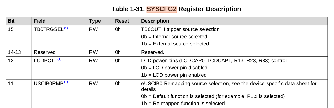
//SYSCFG2|=USCIB0RMP;
UCB0CTLW0 |= UCSWRST;
UCB0CTLW0 |= UCSYNC|UCCKPL|UCMSB;
UCB0CTLW0 |= UCSSEL__SMCLK;
UCB0BR0 = 0x01;
UCB0BR1 = 0;
UCB0CTLW0 &= ~UCSWRST;
UCB0IE |= UCRXIE;
PM5CTL0 &= ~LOCKLPM5;
__bis_SR_register(LPM0_bits | GIE);
return 0;
}
#if defined(__TI_COMPILER_VERSION__) || defined(__IAR_SYSTEMS_ICC__)
#pragma vector = USCI_B0_VECTOR;
__interrupt void USCI_B0_ISR(void)
#elif defined(__GNUC__)
void __attribute__ ((interrupt(USCI_B0_VECTOR))) USCI_B0_ISR (void)
#else
#error Compiler not supported!
#endif
{
while (!(UCB0IFG&UCTXIFG));
UCB0TXBUF = UCB0RXBUF;
}