Hi,
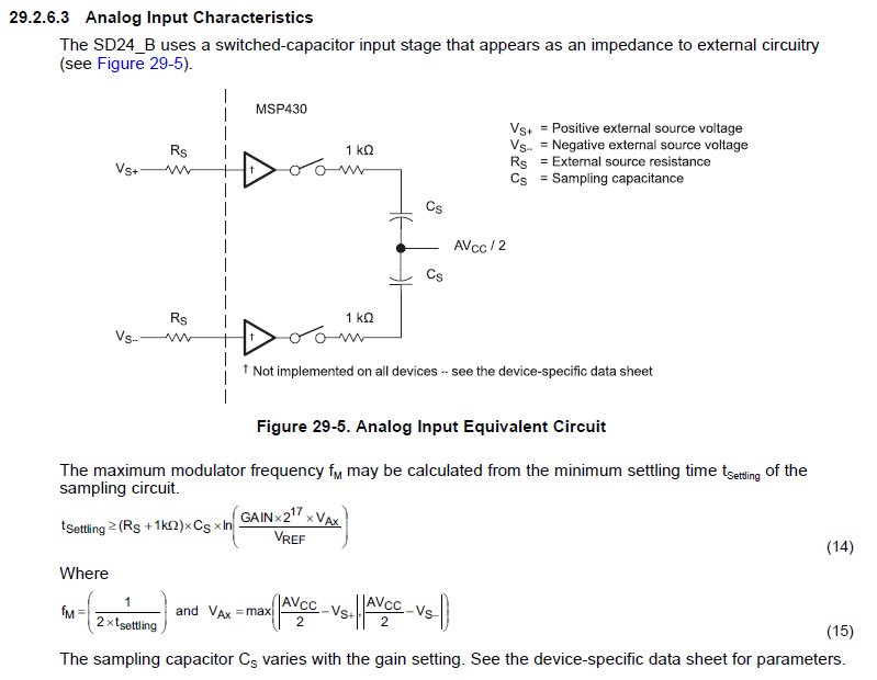
I came across a non-linearity in the SD24 performance.
See below:
ch 0
| ADC reading (dec) | ADC reading (dehex) | Vref | Vin (mv) | ADC/Vin | ADC/Vin/Vin(1) |
| 12784781 | C3148D | 1.24 | 640 | 19976 | 1.00 |
| 13817630 | D2D71E | 1.24 | 790 | 17491 | 0.88 |
| 14840565 | E272F5 | 1.24 | 956 | 15524 | 0.78 |
| 15713836 | EFC62C | 1.24 | 1084 | 14496 | 0.73 |
| 15974404 | F3C004 | 1.24 | 1123 | 14225 | 0.71 |
| 16066820 | F52904 | 1.24 | 1170 | 13732 | 0.69 |
It looks as if the ADC/Vin is not constant as should be, but kind of reduces as Vin is higher (see above)
Vin was measured with DMM on the MSP input.
See below the register dump:
Reg Group Reg Name Reg Value (Hex) Value Meaning
SD24BCTL0 0x1B10
SD24DIVx 3 3
SD24PDIVx 3 8
SD24CLKOS 0 fM
SD24M4 0 fM=fM=fSD24
SD24SSEL 1 SMCLK
SD24REFS 0 Ext Ref (In released SW: internal. Short between internal and ext)
SD24BCTL1 0x802
SD24DMAx 0b1000 SD24TRGIFG triggers DMA
SD24GRP3SC 0 No conv_start for group 3
SD24GRP2SC 0 No conv_start for group 2
SD24GRP1SC 0 Start conversion for group 1
SD24GRP0SC 0 No conv_start for group 0
SD24BIFG NA (read only interrupt status)
SD24BIE 0x4
SD24IE2 1 Converter 2 interrupt enable
SD24IE0,1 ; SD24OVIE2..0 0 No overflow interrupts enabled, no converter 0,1 interrupts enabled
SD24BIV NA (Read only)
SD24BCCTLx 0x000B
SD24MC 0 Bitstream synchronous to fM. Output data changes with falling clock edge, input data is captured with rising clock edge.
SD24DI 0 Bitstream from modulator fed into digital filter
SD24DFS 0 SINC3 filter
SD24CAL 0 Calibration disabled.
SD24SNGL 0 Continuous conversion mode
SD24ALGN 0 = Right-aligned. LSB of filter output is bit 0.
SD24DF 00b Offset binary
SD24SCSx 101 Group 1 - Start of conversion defined by SD24GRP1SC bits in register SD24BCTL1
SD24SC 1 NA: Conversion ongoing indication
SD24BINCTLx 0x0
SD24INTDLYx 00b Fourth sample causes interrupt
SD24GAINx 000b Gain = 1
SD24BOSRx 0xff
SD24OSRx 0xff Oversample = 255+1 = 256
SD24BPREx 0x14
SD24BPREx 0x14 Digital filter preload value = 0x14 = 20
The outputs of the ADCs (SD24 0 to 2) is sampled in rate of 25Hz.
Can you advise as for the reason of the non-linearity?


