


Hello,
Our customer has an question for AGND and DGND separation.
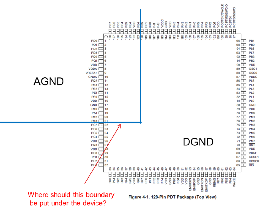
From the pin layout of this device, ADC part and other digital part looks clearly separated inside the device.
So my customer is considering to separate AGND area and DGND area like the below.
Is this way effective in this device?
If it is effective, could you give me some advice where they should put the boundary between AGND and DGND under the device?
Regards,
Oba

