This thread has been locked.

If you have a related question, please click the "Ask a related question" button in the top right corner. The newly created question will be automatically linked to this question.

MSP430F2618: Flash Data Retention

Part Number: MSP430F2618

Flash charge retention is the ability of the flash cell to retain its programmed value during long-term storage. Here, "programmed" means logic 0? 

But I'm confused by the descriptions below, e.g. "leakage only can flip an erased cell with the logic level 1 to a programmed cell with the logic level 0".

  • Hello,

    You must be looking at the App Note MSP430 Flash Memory Characteristics (Rev. B) (https://www.ti.com/lit/pdf/slaa334). 

    user1407287 said:
    Here, "programmed" means logic 0?

    That is correct as discussed in Section 2. "Simplified Flash Memory Cell" of the document.

    user1407287 said:
    But I'm confused by the descriptions below, e.g. "leakage only can flip an erased cell with the logic level 1 to a programmed cell with the logic level 0".

    As described in section 2 of the app note, by default all the cells are erased and represent "1" and the cells that need to be programmed to "0" are programmed to 0. The leakage only occurs on cells that have a fully charged (positive) floating gate which is a 1. Hence the leakage can only occur on these cells which represent "1". When they are programmed to "0", the floating gate positive charge is destroyed and hence there is nothing to "leak" on those 0s and hence will stay as 0s.

    Hope that helps.

    Srinivas

  • Hi,thank you for your reply. 

    As also described in section 2 of the app note, negatively charging the floating cell means programming this cell which represent "0". 

    Why does the leakage only occur on cells that have a positive-charged floating gate? What about the cells that have a negatively charged floating gate?

    I think only the electrons can move from the floating gate.

  • Hello,

    There is an explanation in the 1st reference (Y. Manabe, Detailed Observation of Small Leak Current in Flash Memories With Thin Tunnel Oxides, IEEE Std 1998, pp 95–99) of the App note on how the electrons are emitted towards the gate causing the charge to be neutralized; in effect causing the charge to leak.

    Srinivas

  • Hi, 

    I downloaded the 1st reference, and found that the description of the leakage mechanism was different.  The different descriptions can lead to opposite leakage failure phenomenon (logic 1 to 0, or logic 0 to 1).

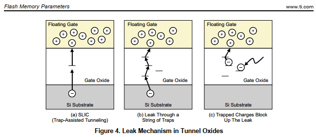
    The description of the App note is as below.

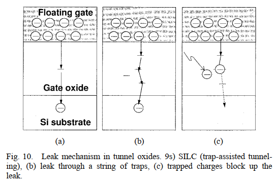
    The description of the 1st reference is as below.

  • Hi, Srinivas,

    Is there any further explanation?

  • Hello, 

    Is there any further information?

  • Hi,

    can you please let us know if the questions are related to ongoing product qualifications on your site or real flash related unexpected behaviors you observed?
    So far I can comment here that the leakage paths documented in the TI application note are historical the ones which were observed when this technology was established and the technology experts compiled this document.

    Especially the effect that tunneling effects caused an erased cell (logical 1 with positive charge on the floating gate) to slowly degrade to a logical 0 by electrons moving via defects (tunnels) to the floating gate. However over the years the technology was significantly  improved to prevent such behaviors. This was proven by multiple process and device qualifications.

    So if you maybe can share some more background on your question TI might be able to help you here better. However we cannot explain or comment on given references not owned by TI. Such a question needs to be asked to the corresponding document owner.

**Attention** This is a public forum