This thread has been locked.

If you have a related question, please click the "Ask a related question" button in the top right corner. The newly created question will be automatically linked to this question.

MSP430F6779:About SD24 SD3

Genius 5320 points
Part Number: MSP430F6779
Other Parts Discussed in Thread: MSP430F6733A, MSP-TS430PEU128

Hi experts,

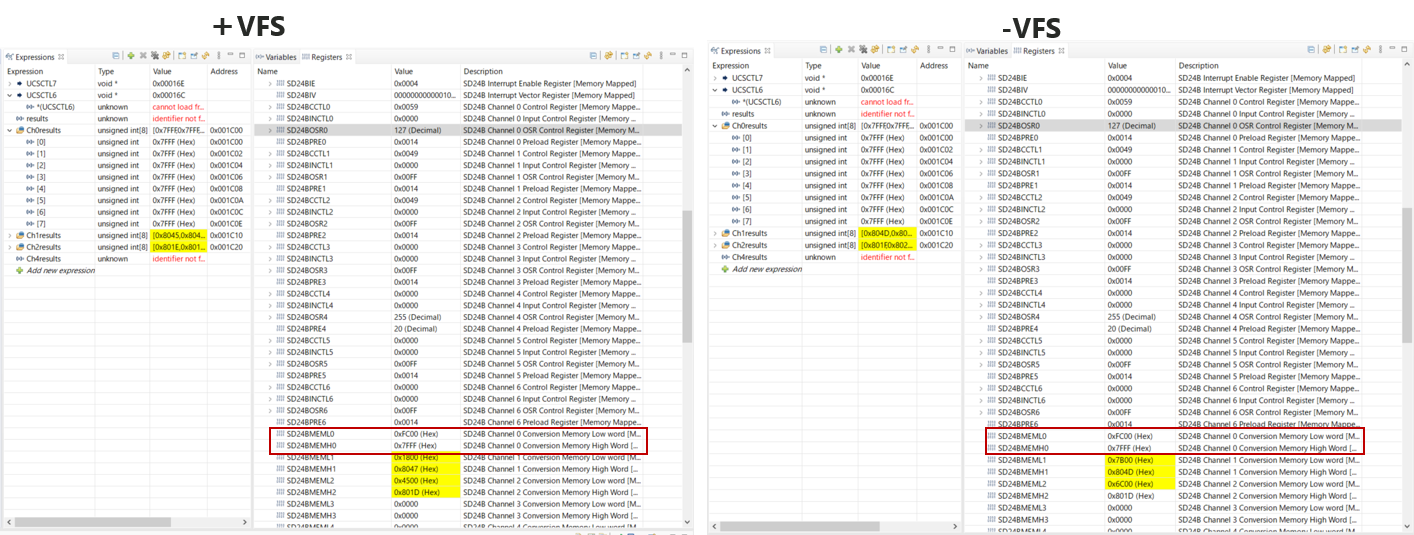
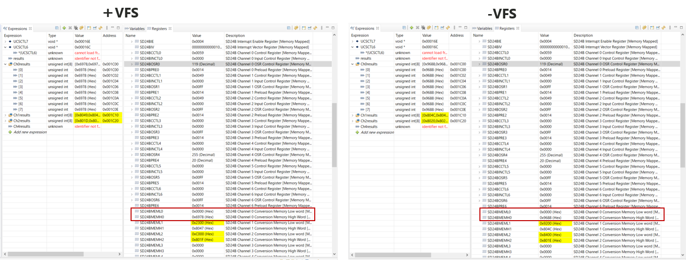
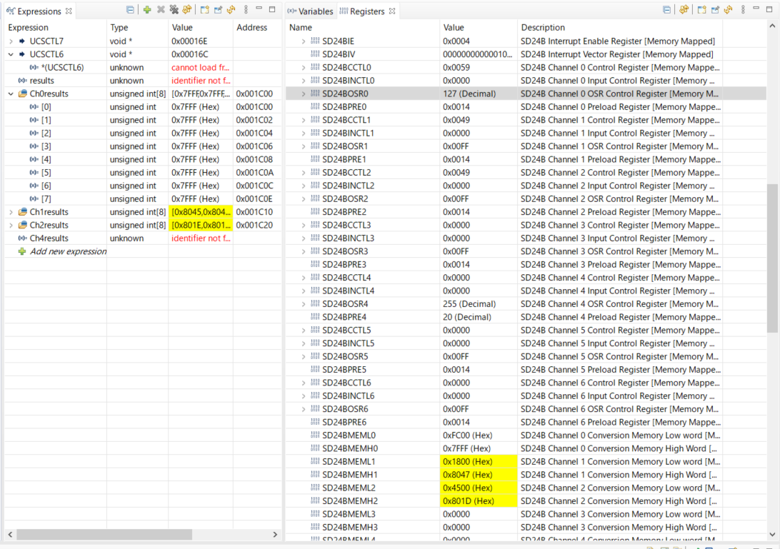
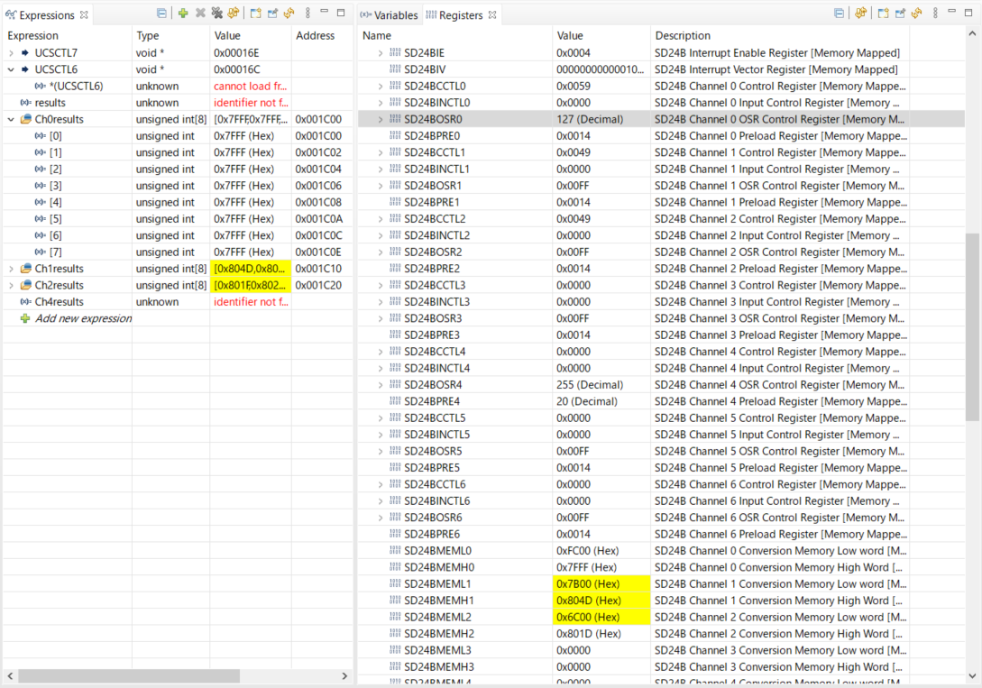
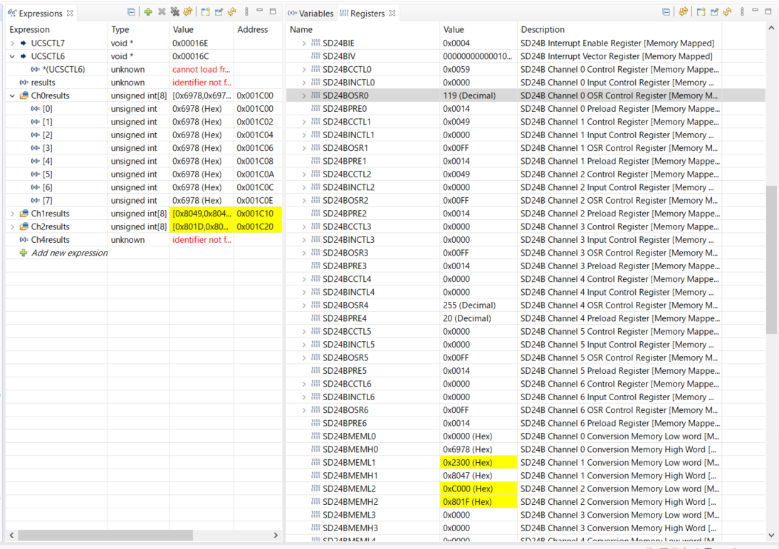
My customer has created two custom sensor boards using MSP430F67719A and MSP430F6733A. Due to the board, there is a case where -VFS (about -1.2V or more) is input to SD24, but SD3 problem occurred because the result is output in two complement mode. The phenomenon is that the result value of +VFS (above about +1.2V) and -VFS (above about -1.2V) are the same. My customer and I have read the errata and know that there is no workaround and that the problem does not occur when using the offset binary mode.

However, according to the customer's research, when the +VFS and -VFS results are far apart, such as when OSR=120, this problem does not seem to occur. To add a little more, the problem seems to occur when the difference between the +VFS and -VFS data results is "1", such as when OSR=128 or 256. I have confirmed the above myself using MSP-TS430PEU128 and F67791A.

Q1: When using two complement mode, can I consider it effective if I set the OSR value such that the difference between +VFS and -VFS is more than 1 (e.g. OSR=120)?
Errata says that the output result will be incorrect regardless of all OSR values and any alignment.

I know that the voltage range that I am inputting in the first place is beyond ±920mV, but it would be great if you could tell me if this is a countermeasure and if it is effective.

Best regards,
O.H

  • Hi,

    Could you add your test code here so that I can check more details?

  • Hi Hawken Li,

    Thank you for your reply.

    The following is the source code when we checked it. We have added the data format and OSR settings to MSP430F677x_SD24B_01.c.
    https://dev.ti.com/tirex/explore/node?node=AA22Oqmq-UUWVa7lCSsBuQ__IOGqZri__LATEST

    #include <msp430.h>
    
    /* Number of conversion results to store */
    #define Num_of_Results 8
    
    /* Arrays to store SD24_B conversion results */
    unsigned int Ch0results[Num_of_Results];
    unsigned int Ch1results[Num_of_Results];
    unsigned int Ch2results[Num_of_Results];
    
    void main(void)
    {
        WDTCTL = WDTPW | WDTHOLD;               // Stop WDT
    
        SD24BCTL0 = SD24REFS | SD24SSEL_1;      // Select internal REF
                                                // Select SMCLK as SD24_B clock source
    
    //    SD24BCCTL0 = SD24ALGN | SD24SCS_4;      // Left-aligned, group 0
        //add
        SD24BCCTL0 = SD24ALGN | SD24DF_1 | SD24SCS_4;      // Left-aligned, group 0
        //
        SD24BCCTL1 = SD24ALGN | SD24SCS_4;      // Left-aligned, group 0
        SD24BCCTL2 = SD24ALGN | SD24SCS_4;      // Left-aligned, group 0
    
        //add OSR
    //    SD24BOSR0 = 127;  //error
        SD24BOSR0 = 119;  //no error
        //
    
        SD24BIE = SD24IE2;                      // Enable channel 2 interrupt
    
        __delay_cycles(0x3600);                 // Delay for 1.5V REF startup
    
        SD24BCTL1 |= SD24GRP0SC;                // Set bit to start conversion
        __bis_SR_register(LPM0_bits | GIE);     // Enter LPM0 w/ interrupts
    }
    
    #if defined(__TI_COMPILER_VERSION__) || defined(__IAR_SYSTEMS_ICC__)
    #pragma vector=SD24B_VECTOR
    __interrupt void SD24BISR(void)
    #elif defined(__GNUC__)
    void __attribute__ ((interrupt(SD24B_VECTOR))) SD24BISR (void)
    #else
    #error Compiler not supported!
    #endif
    {
        static unsigned int index = 0;
    
        switch (SD24BIV)
        {
            case SD24BIV_SD24OVIFG:             // SD24MEM Overflow
                break;
            case SD24BIV_SD24TRGIFG:            // SD24 Trigger IFG
                break;
            case SD24BIV_SD24IFG0:              // SD24MEM0 IFG
                break;
            case SD24BIV_SD24IFG1:              // SD24MEM1 IFG
                break;
            case SD24BIV_SD24IFG2:              // SD24MEM2 IFG
                Ch0results[index] = SD24BMEMH0; // Save CH0 results (clears IFG)
                Ch1results[index] = SD24BMEMH1; // Save CH1 results (clears IFG)
                Ch2results[index] = SD24BMEMH2; // Save CH2 results (clears IFG)
                if (++index == Num_of_Results)
                {
                    index = 0;                  // SET BREAKPOINT HERE
                }
                break;
        }
    }

    With OSR=128, +VFS(SD0N0=GND, SD0P0=+1.5V)=0x7FFFC000, -VFS(SD0N0=-1.5V, SD0P0=GND)=0x7FFFC000.
    I think the theoretical values would be +VFS=0x7FFF FC00 and -VFS=0x8000 0000.

    However, with OSR=120, +VFS(SD0N0=GND, SD0P0=+1.5V)=0x6978 0000, -VFS(SD0N0=-1.5V, SD0P0=GND)=0x9688 0000.
    I think the theoretical values would be +VFS=0x6978 0000, -VFS=0x9688 0000.

    The image quality may be poor, so I have attached a capture screen.

    Best regards,
    O.H

    • OSR=128, +VFS

    • OSR=128, -VFS

    • OSR=120, +VFS

    • OSR=120, -VFS

  • Hi, 

    It seems to be a countermeasure. We will do more internal checking and feed back to you later. 

    Later I will let you know the progress from our side from message.

    I will close the session now.

  • Hi 

    Thank you for your support.

    I hope this one will be a countermeasure and help everyone else.

    Best regards,
    O.H

**Attention** This is a public forum