This thread has been locked.

If you have a related question, please click the "Ask a related question" button in the top right corner. The newly created question will be automatically linked to this question.

MSP430FG4617: ADC mesure

Part Number: MSP430FG4617

Hi!

I have an application where I need to use the ADC of the MSP430FG4617.

The problem is that I'm not having the stabilty that I need. I have a PCB with the uC soldered and I'm testing it with no other components or modules.

As the input signal for the ADC I'm using the A0 channel (P6.0) wich is connected to a 20k potenciometer

Debugging the program and seing the memory register for the ADC, I notice that the value varys in 1, 2, max 5 bits (ocational 10bits jumps) in each iterations.

The funny thing is that I mesure with a tester the voltage of the AO signal and it's stable, barely 0.1mV variations. I tried to filter the signal with a 100nF capacitor and the result was the same.

The program is the following:

void main(void)
{

WDTCTL = WDTPW + WDTHOLD; // Stop watchdog

FLL_CTL0 |= XCAP18PF;
P6SEL |= 0x01;                                // Enable A/D channel A0
ADC12CTL0 = REFON + REF2_5V + ADC12ON + SHT0_2; // turn on 2.5V ref, set samp time

ADC12CTL1 = SHP;                       // Use sampling timer
ADC12MCTL0 = SREF_1; // Vr+=Vref+

for (i = 0x3600; i; i--);                      // Delay for needed ref start-up.

                                                       // See datasheet for details.

ADC12CTL0 |= ENC;                     // Enable conversions

ADC12CTL0 |= ADC12SC;            // Start conversions
while (!(ADC12IFG & 0x0001));     // Conversion done?

__no_operation();                          // SET BREAKPOINT HERE

while(1);

}

Any tips for this??

Thank you!

Regards,
Pedro.

  • Hi Pedro,

    What voltage are you trying to read?  Sensor output, battery voltage, etc.

  • > ADC12CTL0 = REFON + REF2_5V + ADC12ON + SHT0_2; 

    One of the hazards with using a pot for an ADC input is that it's very easy to set the source impedance very high. At 20k, my spreadsheet says you need at least 4us of sample/hold, and SHT=2 (16 MODCLKs) you're only getting about 3us. This is one sort of symptom you get if your sample/hold time is too short.

    As an experiment, try setting SHT very high, e.g. SHT0=6 (128 clocks) and see if it makes a difference.

  • Hi!

    Thank you for your answer

    I tried that but the results still the same. I get 1,2 or 3 bits variations.

    I even set SHT0_15 to have 1024 clocks of sample/hold time

  • The power comes from the debugger (5V) and Im connecting the potenciometer between GND and 5V.

    This is the line A0 (analog input 0) that I'm trying to read

  • The next experiment is probably to run the ADC repeatedly, in a loop, to see if you still see large variations.

    I'm wondering if the reference is taking a long time to settle -- it can take up to 17ms [Ref data sheet (SLAS508J) Sec. 5.29].

  • Hi Pedro,

    Are you still having trouble?

  • Hi Dennis.

    Sorry for the delay. I appreciate your attention.

    I didn't solve this but I stopped doing test. I tryied:

    * increasing sampling time

    * giving more time to Vref to establish

    * filter the signal with a 100nF capacitor

    * reading continously in loops to see more data

    But I still encounter 2,3 .. 5 bit variations

    The funny thing that I tryed using one example code for reading the internal temp and I still see the bits variations (with the potencionmeter disconnected).

    I wonder now if it's a DGND | AGND problem. High speed digital signals interfiering on the analog circuits. Could it be?

    Thanks!

  • Hi Pedro,

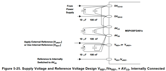
    Yes, it is possible to have interference.  You indicated that you don't have anything else on the PCB, so that eliminates noise from other circuits.  What are you using for bypass/decoupling caps on VDD and AVCC?  Do you have a large ground plane on the same layer as the MSP430 and one below underneath.

    You are welcome to share your schematics and gerber files.

  • Hi Dennis. I'm attaching the gerber files + schematic. There are many other components on the PCB but none of those are in use for this test. I mean, all I/O signals of the board are disconnected and no programmed in SW.

    There is no ground plane, only traces.

    Also, AGND is not connected to DGND close to the uC MSP430 as it should be. For this matter, I tryed to connect it manually by soldering a little wire between AGND and DGND from the bypass capacitors.

    These bypass capacitors are 4.7uF (ceramic). I saw on the datasheet an aditional 100nF bypass capacitor for VDD and AVCC, are these really necesary?

    Thanks!

    FM-500V1R4R2.rarfm-500 V1R4R9.pdf

  • Hi Pedro,

    Unfortunately I can't read the gerbers.  Can you put gerbers in PDF format?

    Regarding the 100nF bypass capacitors on VDD and AVCC, absolutely yes. Note comment from datasheet section 5.9

    Regarding connecting AGND to DGND see this E2E posting.

    Capacitors and connections should be as shown here, otherwise there is no guarantee you will get the performance specified in the datasheet.

  • Hi Pedro,

    It's been a while since we have heard from you, so I'm going to assume you were able to move forward with your project.


    I will mark this posting as RESOLVED, but if this isn’t the case, please click the "This did NOT resolve my issue" button and reply to this thread with more information.


    If this thread is locked, please click the "Ask a related question" button, and in the new thread describe the current status of your issue and any additional details you may have to assist us in helping to solve your issues.

**Attention** This is a public forum