This thread has been locked.

If you have a related question, please click the "Ask a related question" button in the top right corner. The newly created question will be automatically linked to this question.

CAPTIVATE-FR2676: Bug to Generate PWM signal from TA3

Part Number: CAPTIVATE-FR2676

Hello support Team,

Our project is based on the software architecture of the example TI "« \CapTIvateDesignCenter\example_projects\CaptivateDesignCenterWorkspace\TI_Examples\FR2676_CAPTIVATE-BSWP »".
- The configuration chosen in the "CaptivateDesignCenter" is "I2C_Bluck" in the "Communication interface" tab.
- We have configured the Timer A3 setting as follows: P4.5 associated to TA3.2 en PWM mode (perio fixed by TA3CCR0 ), and P4.6 associated to TA3.1 en PWM mode also (perio fixed by TA3CCR0 ).
- Notice that Timer2 has the same configuration.

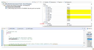
During the execution of the code, we notice unexpected behavior of Timer 3. In fact,in debug mode, its settings (TA3CTL, expected: 0x0111 like TA2, found 0x0131!)
Is modified and its initial configuration is lost with each passage of the function CAPT_appHandler () which is in the while (1) loop of the main ( as follow ) :
 

Questions 100
* Is the “CAPT_appHandler ()” responsible for this change?
* How can we ensure that our Timer 3 configuration is not lost and remains frozen?

Thanks for your response
  • Hi,

    Dou you test the function in free run mode?
    And  could you upload the confirguation code for TimerA3?

    Thanks!

    Best Regards

    Johnson

  • Hello,

    I tested in release mode, but it still does not work.
    The configuration code for Timer3 is :
    // In Init
    SYSCFG3 |= TA3RMP;

    // P4.5 ==> PWM_SPARE1 ( TA3.1)
    P4DIR |= BIT5; // P4.5
    P4SEL0 &= ~BIT5;
    P4SEL1 |= BIT5; // P4.5 options select

    // P4.6 ==> PWM_SPARE2 ( TA3.2)
    P4DIR |= BIT6; // P4.6
    P4SEL0 &= ~BIT6;
    P4SEL1 |= BIT6; // P4.6 options select

    // Disable the GPIO power-on default high-impedance mode to activate
    // previously configured port settings
    PM5CTL0 &= ~LOCKLPM5;
    .....
    .....

    // In execution code
    WDTCTL = WDTPW | WDTHOLD; // Stop WDT

    // Timer 2 & 3 période
    TA3CCR0 = 167-1; // PWM Period


    TA3CCTL1 = OUTMOD_7; // CCR1 reset/set ==>LED_Spare_3
    TA3CCTL2 = OUTMOD_7; // CCR1 reset/set ==>LED_Spare_4


    TA3CCR1 = 0;
    TA3CCR2 = 0;

    // Timer A3 configuration
    TA3CTL = TASSEL__ACLK | MC__UP | TACLR; // ACLK, up mode, clear TAR

    __bis_SR_register(LPM0_bits); // Enter LPM0


    // Then, I change TA3CCR1 & TA3CCR1 from 0 to (167-1) to modify duty cycle

    Thanks,
  • Hi,

    For generate PWM via Timer, you can refer this example code:

    https://dev.ti.com/tirex/explore/node?node=AO9o3LoG1s2mdi4Rrq5Ckg__IOGqZri__LATEST

    And I find Pin4.5 is TA3.2.

    Best Regards

    Johnson

**Attention** This is a public forum