This thread has been locked.

If you have a related question, please click the "Ask a related question" button in the top right corner. The newly created question will be automatically linked to this question.

TM4C1299NCZAD: Influence on VDDC when the rise rate of VDD power input is slow.

Part Number: TM4C1299NCZAD
Other Parts Discussed in Thread: MAX3232

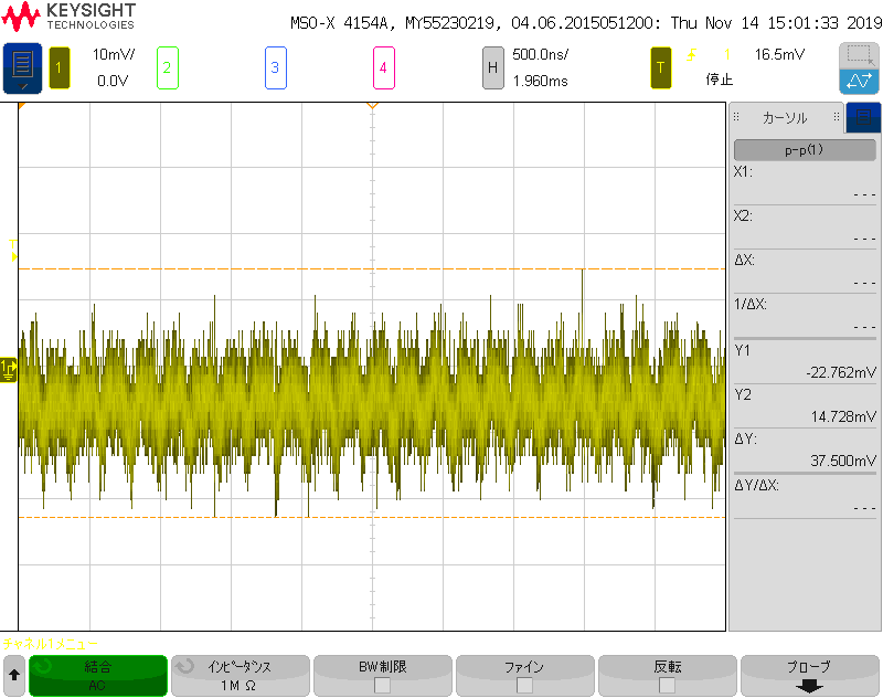
When VDD and VDDA are connected to the same power supply, VDDC begins to be generated when VDD reaches about 2.5V when the power is turned on.

If the rise rate of VDD is very slow, even when VDDC reaches 1.2V, VDD remains at about 2.5V.

Is this situation not adversely affecting the internal power supply circuit?

Although the mysterious burning of TM4C1299NCZAD continues, it is known that there is no problem with the external circuit.

I suspect that this situation is adversely affected.

  • Hello, I am honestly not entirely clear what the background is here regarding this question so I may not be seeing the big picture that you are. From what is described, I don't see how a slow rising VDD/VDDA would consequentially impact the bring up of VDDC at all. Nothing in the datasheet indicates there could be an issue from what I read. If there you disagree, can you point me to the section that is causing this concern? Beyond that, if there is more background here, please share it and maybe I can give a more detailed analysis.
  • As far as I have examined, neither the data sheet nor the system design guidelines nor the silicon errata describe the possibility of chip burning due to the relationship between VDD / VDDA and VDDC.

    I made three types of printed circuit boards with the same peripheral circuit using TM4C1299NCZAD, but mysterious burnout is caused by two types of printed circuit boards where VDD / VDDA is connected to the same power supply and rises slowly.
    However, burnout does not occur in one type of printed circuit board in which VDDA rises after VDD.

    Since the difference is about the voltage of VDD / VDDA when VDDC is generated, I thought there might be a limitation of the VDDC power supply that has not been clarified.

  • user6220457 said:
    Although the mysterious burning of TM4C1299NCZAD continues, it is known that there is no problem with the external circuit.

    Greetings,

    May it be asked:

    • "Just how, 'Is it known' - that the 'Slow Rise' power supply" - causes 'No Problems?'     
    • What is the measured, 'rise rate of VDD' - presented above as, 'very slow?'
    • Is there 'justification' for other than, 'normal/customary' power supply rise rate?
    • Would not your (temporary) replacement of the 'Slow Rise' supply w/a 'More Normal One' - provide further (most necessary) insight?

    From experience - such 'unusual' power supply performance (may) indicate the presence of, 'Voltage Transients' (especially at Turn-On) - which exceed the MCU's specifications - and are 'Known MCU Killers!'

  • Hello,

    I also would like to get the answers from cb1's list of key questions, so please take time to address them as well.

    In addition, I would like to understand more about this burnout case when it occurs.

    • Have you identified the pins that are faulty?
    • And if so, what behavior are you seeing on them?
    • Is it power pins specifically that are damaged, and if so, which ones?

    Lastly, can you share waveforms for the VDD/VDDA rise that is supposedly a cause of this problem?

  • user6220457 said:
    Although the mysterious burning of TM4C1299NCZAD continues

    Does not equal 'mystery' befall the (always) 'helpful:'

    • Number of custom boards suffering from such 'burning.'
    • Population of the board build (i.e. 5, 25, 100 etc.)
    • 'Outside World' (i.e. off-board) connections to 'other' boards and/or electronics

    It proves useful if this list is amended to the one provided for you earlier along w/Vendor Ralph's probing.

    Note too that a 'Slowed 3V3 Rise' - may not be 'appreciated' by other ICs/devices on your custom board - & should those have become damaged - and 'connect to your MCU' - issues (i.e. 'burning') may result... 

    And finally - as a, 'Sanity Check' - this vendor produces, 'Tens of Thousands of these MCUs.'     You should  properly  'compare/contrast'  the  'MCU's, Design, Development, Production' excellence ... with that of your, 'Unnamed, slow-rise, (apparently) troublesome power supply.'      'David' - only rarely - beats 'Goliath' - and it is almost certain - this is not  one of those occasions...    (Odds are high on a, 'Flawed power supply and/or board irregularity' - focus there appears a, superior direction...)

  • Thank you for your answers.

    I am impressed that you are thinking seriously.

    I'll give you a little more specific information.

    ・5V is generated from 24V with APXW005A0X3-SRZ (ABB Embedded Power), and 3.3V generated with EN5337QI (ALTERA) from this 5V is input to VDD / VDDA.

    ・The same 3.3V is used as the power supply for CPU peripheral circuits.

    ・The same 3.3V is connected to VBAT,VREF+.

    ・The 3.3V (VDD) output rate of EN5337QI is set to 0.003V/us so that the VBAT rise rate is less than 0.7V/us.

      This is in accordance with ELEC # 02 of Silicon Errata “Tiva ™ C Series TM4C129x Microcontrollers Silicon Revisions 1, 2, and 3”.

      The silicon revision is 3.

    ・3.3V (VDD) starts to be output when the 5V input reaches about 2.15V, but since the 5V rise rate is 0.00026V/us, 3.3V (VDD) rises to about 2.35V. 3.3V (VDD) catches up to 5V input.

      After that, 3.3V (VDD) rises at the same rate as 5V input.

    ・VDDC starts to rise when VDD is 2.36V and reaches 1.2V when VDD becomes 2.39V.

    ・The two burned CPUs were analyzed by TI, and the result was that the device was exposed to voltage conditions outside the specified range of use.
     (QEM-CCR-1906-01054)
       "TI electrical testing verified the issue and the root cause was determined to be Electrically Induced Physical Damage (EIPD).

        Electrical testing of the customer return units found several pins with Opens/Shorts fails.

        This supports the external damage noted on the package.

        Data indicates that the devices were subjected to a voltage condition outside of the specified usage range."

    ・However, all power pins (VDD, VDDA, VBAT, VREFA +) are connected to 3.3V of EN5337QI output, and all GND pins (GND, GNDA, GNDX, GNDX2, VREF-) are connected to 0V.

      Also, since the peripheral circuit is driven at 3.3V, which is the same as VDD, it is unlikely that a voltage exceeding the maximum rating will be applied to the IO pin.

    As a result, I have stopped moving forward.

    blue:+5V

    yellow:3.3V(VDD)

    green:VDDC

  • I will explain the situation.

      Board A: 7 out of 45 boards burned or malfunctioned.

      Board B: 3 out of 17 boards burned or malfunctioned.

    thank you

  • Hello,

    Thank you - your presentation of such exhaustive data is both welcome & much appreciated.   Your inclusion of the, 'KEY Voltages at Power-Up' (via scope cap) proves especially useful - well done!

    I will follow your order of presentation:

    "3.3V generated with EN5337QI (ALTERA) from this 5V is input to VDD / VDDA.

    You meant, "3V3 is input (not 5V) to VDD/VDDA" - did you not?

    " two burned CPUs were analyzed by TI, the result was that the device was exposed to voltage conditions outside the specified range of use."

    This was as I had earlier suspected.

    "Electrical testing of the customer return units found several pins with Opens/Shorts fails."

    This is unfortunately  vague!    Did not the vendor analysis 'identify' those 'damaged pins?'    Especially useful would be, 'Power Pin failures' - yet such is (apparently) 'unknown!'    Should, 'Non Power Pins' (i.e. ideally GPIO) have been found 'faulty' - tracing them to their, 'Peripheral Sources' - proves (highly likely) to have identified your, 'Fault Agent!'

    "since the peripheral circuit is driven at 3.3V, which is the same as VDD, it is unlikely that a voltage exceeding the maximum rating will be applied to the IO pin."

    May I note that 'unlikely' does not rise to, 'Never!'     Usually - it is my firm's finding - that, 'Peripheral chips prove more robust' than their, 'MCU counterparts!'    (from ALL Vendors - this likely due to the greater complexity (thus vulnerability) embedded w/in the 'mixed signal MCU.')

    Preliminary Conclusions:

    • Your report of, '15% of Board A' & '17% of Board B' suffering failures is 'most serious' - & 'Far exceeds Vendor 'Norms!'
    • It is suspected that, 'Somewhere w/in the MCU 'Handling, Assembly, & Testing Process' - ESD events (may) have occurred.   Have you, 'Adequate & Active' ESD Management - throughout your system?
    • In addition -  the 'Quality & Reliability' of your 'board build' is unknown.   Was this done by a 'proven' facility?
    • While we (now) know the 'Number & Percent of Failures' - we do not know, 'When/Where they may have occurred' w/in your multiple processes.    Have you such knowledge?
    • Perhaps a 'long-shot' - our TM4C1294 MCU Manual (Not the same as your 1299!) notes, "a.  To ensure proper operation, VDDA must be powered up before VDD if sourced from different supplies, or connected to the same supply as VDD.  There is not a restriction on order for powering off."    (I've only access to that manual as I'm travelling.)    Should there be, 'Significantly Greater Capacitance and/or Inductance - at/around (or 'felt') by the MCU's VDDA pins - this specification (may) not be met.   (VDDA's arrival will be 'delayed.')     [this from Table 27.6, TM4C1294 manual]
    • By 'my read' of your Scope Cap - 'All is well.'    Vendor Agent proves far more experienced to 'confirm or negate.'
    • Should the 'Peripheral Chips' connect to the MCU via, 'Long, Narrow, Direction Deviating or 'via'ed' traces' - the unwanted, resulting, 'Inductance introduced'  (may) be sufficient to cause a brief (transitory) Damaging Over-Voltage!
    • It is suggested that you, 'Clearly Mark & Quarantine' ' those boards which contained, 'Failed MCUs'     Vendor's MCU is 'most unlikely' to have caused, 'Failure at the rates you noted!'    These boards - and/or their build - should be 'exhaustively reviewed' for:
      • 'board build defects'
      • and/or 'mismarked or incorrectly valued components'
      • and/or 'misplaced components'
      • along w/a 'serious via check' - especially if the board is 'multi-layer'  
      • AND a proper, 'Survey & Check' of each/every component (especially ICs) enabled to 'Connect to the MCU!'    A failure by one of these, 'Non-MCU devices' may have impacted your MCU!   (i.e. Casting Blame - entirely/only upon the MCU - may be premature & falls short of a, 'full/proper' Failed Board Analysis.

    Hopefully something herein proves 'Guiding and/or otherwise useful' - such is our objective...    Best of luck - and (perhaps further) analysis...

  • Hello,

    I review the QEM report, thank you for sharing the exact one as I do have the ability to look it up.

    Based on the findings in the report, and the voltage ramp image posted above, I am seeing no reason to come to any sort of conclusion that VDDC is impacted by VDD/VDDA slow rise time in the way you have stated, or that you have uncovered an unknown errata item for the device. I'm honestly a bit perplexed where the idea of that possibility came from as nothing in the report would indicate to me to even look in such a direction.

    I don't want to share details of the report on here to protect confidential information, but I have seen nothing that calls into question the conclusions from it that this is overvoltage situation.

    I would recommend you read through cb1's commentary on how to try and debug this further at a system level - he has given many points of good advice.

  • The note “VDDA must be powered up before VDD” written in the TM4C1294 MCU Manual could also be found in the TM4C1299 MCU Manual.

    I missed this note completely.

    The reason why the rise timing of VDDC was suspected was because there was no burnout failure on the board where the rise of VDDC was sufficiently slower than the rise of VDD.

    Review the peripheral circuit and look for the possibility of overvoltage.

    Thank you everyone.

  • user6220457 said:

    The note “VDDA must be powered up before VDD” written in the TM4C1294 MCU Manual could also be found in the TM4C1299 MCU Manual.

    I missed this note completely. 

    Indeed - finding that required (some) 'digging.'   (You addressed the vendor here - yet it was young, 'Non vendor staff' - which, 'Made such find.')

    user6220457 said:
    there was no burnout failure on the board where the rise of VDDC was sufficiently slower than the rise of VDDC.

    You may wish to 'edit/correct' that sentence.

    Somehow 'everyone' seems unlikely to 'see/hear' such 'thanks' - two here (alone) have 'earned that!'

  • By the way, what kind of inconvenience will occur if VDDA does not rise before VDD?

  • user6220457 said:
    By the way, what kind of inconvenience will occur if VDDA does not rise before VDD?

    As that direction stemmed from an MCU note (earlier listed & identified) - it 'falls upon the vendor' to properly detail.

    However - I would (almost) 'bet the farm' that your scope cap, 'Could be improved.'    Your Scope Probes should be (properly), 'Placed at the actual, specified MCU pins' - not at some random (i.e. more convenient) junction!     In addition - the scope's ground leads should be removed - and each probes' (now exposed) ground body - should contact a 'nearby' board ground point - via a, (very) short & direct 'wrap-around' connective lead.   

    Such will enable the 'purest of measurements' - the excessive 'lead length' imposed by the 'normal' scope ground leads introduces 'unwanted, even erroneous signal couplings' - none proper and/or potentially 'masking' your scope's (desired) captures...    A supporting/clarifying photo follows:

  • May it (again/Sigh) be noted - that, 'Poster has 'Verified his own post' ... Not the one which 'Best Identified & Lead the Way' to Poster Success!

    As stated (here) many times - the, 'Use of 'Verify' proves unfortunate - as indeed that, 'IS the action which the poster IS TAKING!'

    Alas - those 'deep diving' in posters' (many posters) behalf - receive 'No Benefit' - when 'their work passes w/out GREEN REWARD!'    Such proves (very) FAR - from motivational...

    A superior 'direction' for posters would result from, 'This Post Resolved my Issue' button - of course 'marked in GREEN!'

  • Hello,

    user6220457 said:
    By the way, what kind of inconvenience will occur if VDDA does not rise before VDD?

    It's not fully specified which tells me that the array of results could vary.

    My guess for most common issue is that since VDDA sources the clocking circuitry, you'd have parts of the device try and start before* the clock and the device would not work as a result.

    VDDA must be supplied with 3.3 V, or the microcontroller does not function properly. VDDA is the supply for all of the analog circuitry on the device, including the clock circuitry.

    However, given the statement as it is made, it is certainly possible to me that electrical damage could occur to the device as well.

    I wish I had a clearer answer, but usually these statements are left broad intentionally as there can be multiple failure points when the spec is violated and we may not be able to characterize all possible points of failure that could occur.

  • I am sorry.I didn't know how to use the post.

    In addition, there are many problems such as google translation that makes the content of the post a little different from the original intention, or that the answer you received becomes an unknown sentence.

    Thank you for answering my question many times.

  • There is a great possibility of overvoltage from outside the MPU, but in addition, there seems to be a big problem in connecting the same power supply to VDD and VDDA.

    It was very helpful.

    Thank you very much Ralph Jacobi and cb1.

  • Thank you - please do 'Scroll Back' & confirm your understanding of, 'Scope Probe Usage' - which I illustrated w/a 'Close Up Photo' - as well...

    All of your probes should:

    • have their ground leads (temporarily) removed
    • employ the (proper) wire loop Ground Method (shown in the photo) tied to a pcb ground point as close as possible to 'VDD, VDDA & VDDC.'    (You'll need a 'helper' - and/or another hand - to manage 3 Probes at once.
    • Setting your Scope's Horizontal Sweep - at/around  '1-2 µS' per division - is 'Far More Likely' to 'Reveal the (likely) Transient Voltage Spikes' - which 'KILL MCUs' w/Alarming Regularity...

  • I've posted the VDD, VDDA, and VDDC waveforms using the scope probe as a wire loop grounding method.
    ●VDD
    ●VDDA
    ●VDDC
    No abnormal spike was observed for VDD,VDDA,VDDC.
    I think GPIO input may need to be considered.
  • Thank you -  your extra time/effort (both) helpful & appreciated.

    To your Scope Caps:

    • Due to the  (assumed) 'shortage of hands' - ONLY a single channel appears w/in each Cap.    While that 'has value' - the 'Comparative View of  the RISE of VDD & VDDA' (w/in the same Cap) - would prove insightful - would it not?    Especially as the removal of the 'overly long Probe's Gnd. lead' now enables a 'truer view' as 'extraneous Noise Pick-Up' should have been reduced.
    • Staff questions if the 'Cap they've marked-up' - may reveal (even)  'A higher Amplitude Spike' - if you, 'Switched your Horizontal Sweep to 100nS/Div or even 50nS?     (much 'energy' is 'hinted at' via your 'existing Cap' - wise to 'probe again as directed.')
    • And - might you confirm:
      • all of your earlier Scope Caps (i.e. many posts before) resulted from your, 'Probing from 'Points of Ease/Convenience' - NEVER from the ACTUAL 'VDD, VDDA or VDDC' MCU PINS!
      • your NEW Scope Caps resulted from your (modified) Scope Probe's (i.e. Leadless) 'Directly Contacting the MCU's (VDD, VDDA, VDDC) PINS!'   (even though - this proved 'inconvenient!')

    Follows your Cap - 'marked up by Staff' - indicating their, 'Points of Interest.'    Both Polarities of Transients should be 'more expansively reviewed' - either may provide a 'Death Blow to hapless MCU.'    (Note that Staff are superb @ Math & Programming - immersed now w/in Electronics/MCUs - and share 'cb1's curse' as, 'Failed Artists.')

  • Thank you cb1.

    The previous capture was a measured waveform from a check terminal located about an inch away from the MCU.

    The new capture is the measured waveform from the nearest via on the back of the MCU.

    The detailed waveform of VDDA spike is put.

     VDDA(Long afterglow)

  • user6220457 said:

    The previous capture was a measured waveform from a check terminal located about an inch away from the MCU.

    The new capture is the measured waveform from the nearest via on the back of the MCU.   

    You ARE getting closer to the MCU (staff grants you that) and, (almost) ALL 'Bets are Off' if yours is a BGA device.    In the event that yours is a 'QFP' (leaded device) - we can show you photos revealing, 'How Waveform Damaging - even a 2-3 cm length trace - negotiating a 'via' - can be!'

    With the Scope Caps 'as they are' - belief lessens that the issue is transient arrival upon: 'VDDA, VDDC or VDD.'    That leaves any/all connections between the MCU and other chips - and even 'more highly suspect' - those travelling, 'OFF your Board!'    Those (off board) should receive your full & detailed attention - following that check those, 'Board resident traces of longest length and/or inductance.'

    Keep in mind that (either voltage polarity) - when beyond MCU specification - may prove damaging.   (i.e. you must monitor and/or 'protect against' transient voltages exceeding VDD and/or driving more than a diode drop below System Ground.)

    You've not mentioned - nor have we asked - if 'Power Devices' are, 'On your board' and/or 'Off board' yet interconnected.    These are 'Prime Suspects.'

    We've substantially exhausted the 'MCU Nature' of your thread - much time & effort will be saved if the 'Factory Analysis' provided 'more definitive Pin Damage Identification.'    Suggest that if that was not supplied - perhaps that exists - yet was not shared ... cannot hurt for you to 'nicely' 'Ask for that.'

  • The QEM-CCR-1906-01054 report included the following information about damaged pins:

    Unit 1:-Failed FT1 at RT @ I_B_DieIdShorts_1 @ Pins Test-PC2_TDI_184
    Unit 2:-Failed FT1 at RT @ I_B_DIEID_OPEN_PINS @ Pins Test-PA0_58; PA1_59; PA2_60; PC2_TDI_184

    PC2_TDI was connected to a JTAG connector 0.8 inches away, and the connector was not connected when the printed circuit board was used.No components such as pull-up, pull-down, and protection diode are connected to the TDI signal.
    PA0_58; PA1_59; PA2_60 are connected to the FPGA 1 inch apart, but the IO power (3.3V) of the FPGA is supplied from the same power supply as the MCU.

    Some printed circuit boards that are malfunctioning do not recognize JTAG.
    In some cases, printed circuit boards that have been operating normally in in-house tests before shipment become defective one after another in the field.

    I have recently confirmed that the firmware settings of unused GPIO pins remain the default, or the GPIO input connected to the buffer IC on the circuit diagram is open without the buffer IC being mounted.

    In the field, the weak GPIO may be affected by some kind of electrostatic noise.

    (In this project, I can't directly check the situation in the field.I just guess.)

  • Thank you - the 'plot thickens' w/the arrival of your (greatly) extended data.

    It is hoped that 'vendor agents' might (still) 'visit your thread' - and further clarify their firm's 'QEM-CCR' reportage - especially in light (now) of your 'Failure Data.'   

    Staff & I are 'bothered' by vendor's report stating that 'PC2 (TDI)' is apparently (both):   (you made no comment...)

    • 'Shorted'  "Failed FT1 at RT @ I_B_DieIdShorts_1 @ Pins Test-PC2_TDI_184"
    • and (somehow) 'Open'   Can (both) prove true?   "Failed FT1 at RT @ I_B_DIEID_OPEN_PINS @ ... PC2_TDI_184"
    • in addition - are those '4 pins listed' the, 'Only pins' which vendor 'found and/or deemed' defective?   (that's much to your favor - if true...)

    user6220457 said:
    No components such as pull-up, pull-down, and protection diode are connected to the TDI signal.

    We were taught to (almost) 'Never allow an MCU input to, 'Float!'    You may have 'saved' the cost of an 'smd pull-up R' - yet invited 'trouble.'   It may be possible to 'Add the 'pull-up' at/around the JTAG connector' (importantly Avoiding a 'board-spin') - as both 3V3 & TDI are connector resident.   

    It is unclear if, 'Only PC2 (TDI)' suffered this 'pull-up (savings)' or if the remainder of the JTAG pins (also) were, 'Pull-Up Free.'    A 'more acceptable' means to add those resistors might see you 'Create a, tiny pcb which 'plugs-in' to the (existing) JTAG Connector (and remains there) - thus provides those 'missing resistors.'    (that warrants a 'LIKE' - or another, 'This Resolved' -  if only to recognize 'inspiration' - does it not?)

    As regards 'Failed Pins: PA0, PA1, PA2 - it is assumed they are 'SPI' - is that correct? 

    If that's so:  

    • Are those pins (PA0-PA2), 'Charged w/programming the FPGA?'   
    • Does not the FPGA 'awaken' in a 'disordered' state - and remain so - until the MCU performs (both) its own initialization AND then - FPGA configuration?    The fact that 'so many pins' which are 'common between the MCU & FPGA' - points to (some) likely issue here!    

    user6220457 said:
    (In this project, I can't directly check the situation in the field.   I just guess.)

    May it be noted that my small firm - is 'Even Further Away' - and 'Far Less Able' (than you/your firm) to, 'Know & Check the situation in the Field!'   You or an otherwise, 'Qualified Designee' (may) well consider 'Visiting, Interviewing & Deeply Observing' - so that any/all possible 'Application Risks' are identified - and 'Corrective Actions' (in a detailed writing) can be issued...    Somehow - such seems superior ... to a 'Guess.'

  • (Initial note, please ignore that we suggested the post above as an answer, I was trying to quote and misclicked - the content is far more exploratory in this case)

    Hello cb1,

    cb1_mobile said:

    Staff & I are 'bothered' by vendor's report stating that 'PC2 (TDI)' is apparently (both):   (you made no comment...)

    • 'Shorted'  "Failed FT1 at RT @ I_B_DieIdShorts_1 @ Pins Test-PC2_TDI_184"
    • and (somehow) 'Open'   Can (both) prove true?   "Failed FT1 at RT @ I_B_DIEID_OPEN_PINS @ ... PC2_TDI_184"

    These were two different units, which is why both cases are true.

    I cannot really clarify much else about QEM specifically - I am not an expert with the failure analysis process for one, and also it is not my place to share further details from within the QEM.

    In general. I would usually second that the JTAG circuit should have pull up and pull down resistors. However, depending on trace length, they may not be needed. This is from the System Design Guidelines:

    Tiva™ C Series microcontrollers have default internal pull-up resistors on TCK, TMS, TDI, and TDO signals. External pull-up resistors are not required if these connections are kept short. If the JTAG signals are greater than 2 in. (51 mm) or routed near an area where they could pick up noise, TCK should be externally pulled-up with a 10K or stronger resistor or pulled-down with a 1K or stronger resistor to prevent any transitions that could unexpectedly execute a JTAG instruction.

    The key part here though, that is hard to gauge, is if there is noise present. If so, then the resistors are needed.

  • Ralph Jacobi said:
    the content is far more exploratory in this case)

    Is it not true that (even) greater, 'exploratory' content is that which advises, "External pull-up resistors are not required if these connections are kept short ... or routed near an area whey they could pick up noise."     

    How can the 'Final Location' of the MCU be (always) KNOWN - and is it  'safe & wise'  to 'expect' (really hope) that such location is to (forever) remain 'Noise-Free & unchanged?'     Even when - and especially when - the use of  'RF devices' proves beyond 'widespread!'     What then - such has 'often befallen our clients' - proper 'anticipation & implementation' (i.e. defensive tactics) ALWAYS trumps 'the hope for idealized, forever sustained - operating conditions!'    Apparently the quoted, 'System Design Guide' may (also) be judged as 'exploratory' - and 'wishful!'

    With (many) years of 'real world, Tech Design & Diagnostics' - successful enough to propel a  "Tech firm from 'Start-Up' to PUBLIC Co." - the representation of  'Multiple, often highly caring & technically detailed (many past 'proven') suggestions' as (merely) 'exploratory'  -  registers as 'one man's opinion'  and may be judged as, 'incomplete & often incorrect... '

  • I provided incorrect information about the connection destination of PA0, PA1, and PA2.

    • PA0 and PA1 are connected to an RS-232C driver / receiver IC (MAX3232EEUE +). The MCU and MAX3232 are about 3 inches away.

    • PA2 is open and the firmware has no settings for this pin.

    This printed circuit board may be exposed to noise that adversely affects JTAG and open pins.

    I can't write in detail, but depending on the characteristics of the facility where this printed circuit board is installed, I came up with the possibility of being exposed to noise.

    You may be disappointed, but I don't have much time to investigate, so I want to monitor the situation after following these steps.

    • Pull up / down the JTAG signal.
      TCK, TMS, TDI: Pull up with 10kΩ resistor
      TDO: Pulled down with a 10kΩ resistor

    • Pull up PA0 and PA1 pins with 10kΩ resistor.

    • Set unused GPIO pins to LOW output in firmware settings.

    • Pull up the input GPIO pin connected to the unmounted circuit.
      Pull up with 3.3kΩ or 4.7kΩ resistor.

    I don't think it's enough, but I want to take immediate action without recreating the printed circuit board.

    thank you.

  • Thank you - your responsiveness is welcome & appreciated.

    user6220457 said:
    This printed circuit board may be exposed to noise that adversely affects JTAG and open pins.

    From MANY Years in the Design & Diagnostic 'trenches' - it proves (by far) SAFEST - to, 'Provide for the eventuality of the MCU board being placed w/in a, 'Noise and/or RF-rich' environment.'     The new actions you propose move you in that (preferred) direction.

    user6220457 said:
    TDO: Pulled down with a 10kΩ resistor

    Vendor's Guide directed use of a 1KΩ pull-down.   (we find 2K2-3K3 effective - yet we deploy ARM MCUs from multiple vendors)

    user6220457 said:
    Set unused GPIO pins to LOW output in firmware settings.

    That's one option - suggest that you choose the 'lowest possible' Output Current.    (believed 2mA - in your case)

    user6220457 said:
    I don't think it's enough, but I want to take immediate action without recreating the printed circuit board.

    My group  provided a (pardon) 'Advantaged Suggestion' - which enabled the, 'addition of JTAG resistors' to your 'mating JTAG Connector!'     (resistors mount to a tiny pcb - integrated  to the connector - (that connector 'remains') w/your board.)    This method has been, 'Client  Confirmed & Approved for Field Use' & has proven robust & effective.    (Hacking into existing pcb traces ... Not so Much!)    We are surprised that you (appear) to have 'missed this 'MCU board-spin eliminating' inspired technique!'

    It is believed that the vendor's 'System Design Guide' somewhat encourages, 'Board Designers to forego the use of the (proven Safer) EXTERNAL JTAG 'pull-up/down' resistors!'    Risk-Reward does not favor such 'wishful' guidance.   

    FAR BETTER (perhaps inspired) is to ALWAYS include, 'PCB FOOTPRINTS' for the 'External JTAG Resistors.'   (these resistors may be noted as 'DNF' (do not fill) - yet quickly/easily ADDED - when & as needed!)