This thread has been locked.

If you have a related question, please click the "Ask a related question" button in the top right corner. The newly created question will be automatically linked to this question.

TM4C1290NCZAD: Master Read-access on QSSI

Part Number: TM4C1290NCZAD

Hello Team,

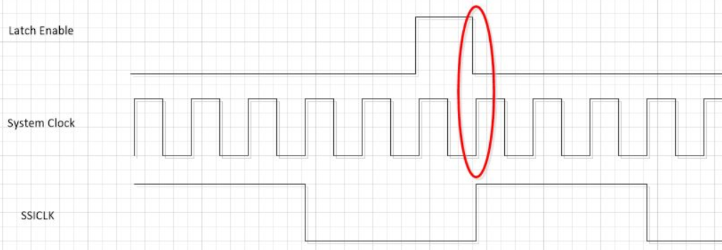
I got inquiry about Quad-SSI from our customer. Customer is developing their system with TM4C1290NCZADI3R, they noticed the refection signal on SSI1Clk(20MHz) line. I attached their captured waveform.(TM4C1290NCZAD_QSSI.pptx) Would you consider there is any issue by this signal?

Also, according to datasheet (Table 26-7. Recommended FAST GPIO Pad Operating Conditions), customer supposes those GPIO has Hysteresis(VHVS : MIN 0.49V), however, customer is not sure how customer should understand this definition. Could you elaborate it, please?

I tried to summarize customer’s inquiries to above pptx file. It is really appreciate if you will be share Expert’s advice / comments on this.

Best regards,

Miyazaki

  • Hi,

       First of all, can you clarify if the MCU is receiving the SSI1CLK or it output the SSI1CLK. In another word, is the MCU the master or the slave? if the MCU is the master then you need to check the Vih of the slave device. If the MCU is receiving the SSICLK as a slave then, do you see any problem sampling the data on the RX? With the hysteresis, I don't think you should have problem with the waveform you are seeing. The Hysteresis will prevent several quickly successive changes if the input signal would contain some noise. The Vih as stated in the datasheet is 0.65*VDD. Suppose the VDD is 3.3V then the Vih is 2.145. The MCU will detect a low-to-high transition at 2.145 V as a valid transition. The 0.49V hysteresis is the voltage band around the Vih that will prevent from recognizing a new transition. 

  • Hello,

    I am customer of Miyazaki san.

    I should have elaborated this question. The MCU is the master.

    1.What I would like to ask is read operation of the master. Can the master latch read data correctly by such a clock wave form? (shown in Miyazaki san's ppt file)

      The clock is reflecting around VIH.

    2. VHYS can be applied to the clock even though the clock is OUTPUT ?

    Best regards,

  • HI, 

      Thank you for your clarification. If there is reflection, it is due to the impedance mismatch between the driver (the MCU SSICLK output pad) and receiver (your external SPI device). You can add series resistor and keep the distance short to alleviate the reflection.

      Can you confirm if you are seeing any issues for the master to sample the RX data correctly?

      Normally the SSI module will use its internal clock (System Clock) to sample the the RX pin. Below is an example internal representation, particular for the master operation. Per your configuration, you have SPO=1 and SPH=1 and SPICLK at 20MHz. The module will use the System clock and the latch enable to latch the RX at the corresponding SSICLK rise edge.  It doesn't really use the SSICLK directly to sample the RX data. The module will drive TX at the SSICLK fall edge. The Vhys does not apply in this case. It is when SSICLK is an input for the slave mode. 

  • Hello Charles,

    My group did not realize that the SPI module so employed the System Clock.   With that said - we are "troubled' by the (implications) of this timing diagram  (reproduced here) & the related description.  

    In the example - and illustrated by the drawing - we believe the System Clock is 6x the SPI Clock.   (meaning that should System Clock be 120MHz then SPI Clock is 20MHz - which agrees w/the description above.)

    Now our concern - and (possibly that of the poster) - is not the System Clock (being (many) multiples of the SPI Clock) - far more vulnerable to "jitter" & (possibly) other timing aberrations?    (we believe that IS the case.)    In addition - as the SPI Clock "rides the (near) identical signal-impedance (pcb) path" as SPI Data - does not that "equality" render the SPI Clock a "superior" clock choice?

    Thinking a bit more - bit deeper - the fact that the SPI Clock must be presented to (and drive the external device(s)) - even though "divided down" in frequency -  likely reduces its ability to produce a "proper square-wave" (at frequencies at/above ~5MHz, certainly 10MHz)!    The System Clock - freed from that "external drive requirement" - may (then) be more "pure" (i.e. square) - thus prove the better choice.    Are we close in this theory ...  even though we shifted 180°?   (Not the 1st time!)   Thanks your time/attention.

  • Hi cb1,

      The source of the jitters is mainly from the OSC. If you check the datasheet it is in 50ppm. The System Clock is what millions of gates in the chip use as the reference clock. For digital design, one of the steps is the physical design STA (static timing Analysis). it is important and recommended to close timing based on synchronous clocks. When you have logic crossing among different clock domains especially crossing between un-synchronous clock domains, you are prone to errors in closing the timing. Errors can be made in the form of declaring false multi-cycle paths. In the past, I do remember only when SPICLK is equal to the System clock frequency will SPICLK directly be used as the clock source to the flops due to the skew between internal clock and the SPICLK on the I/O. 

  • Hi Charles,

    Thanks for clarification. 

    best regards, Miyazaki

  • Hi Charles,

    I close this ticket, but, I received additional question form customer. Please allow to ask this inquiry, sorry.

    Although customer understand this reflection signal could not be any problem, would you consider there is any limitation(Max) for this reflection signal? I believe it is tough to decide this definition. To resolve customer’s concern, it is best way to remove this reflection. But, since customer already created board, it is really appreciated if you will be able to share Expert’s advice.

    (My guess is that, The issue would not occur unless the voltage drops to VIL threshold )

    Best regards,

    Miyazaki

  • Hi Miyazaki-san,

      Earlier I mentioned that reflection was due to mismatch impedance on the transmission line. Reflection noise results when an electromagnetic wave encounters a boundary from one medium to another medium. When the wave hits the boundary, part of the energy is transmitted as signal and part of it is reflected back to the energy source. Maintain consistent impedance on the signal trace, adding a series resistor close to the source and keep short distance on the PCB trace are all methods to reduce reflection. 


  • Hi Charles,

    Charles Tsai said:
    adding a series resistor close to the source and keep short distance on the PCB trace are all methods to reduce reflection. 

    Absolutely!

    Poster's client may also benefit from:

    • avoiding (any) vias on such critical signals
    • minimizing trace's "change of direction"
    • not allowing (other) high-speed and/or high-level signals to come too close
    • when possible - employing a wider (even thicker) trace
    • slowing the SPI clock ... even ("tuning it" to different (lowered) frequencies may "null"  the reflectance/disturbance)

    and

    • avoiding any/all "board to board" transitions of such "critical signals."    (untold if this signal routes "off-board.")

  • Hi Charles

    Customer understand that, they have to obey “Recommended Operating Conditions” and they should remove this reflection.

    But, customer wants to know how much reflection signal would be allowed. Can I have your comments on this, please?

    Best regards, Miyazaki

  • Hi Miyazaki-san,

     Note that Vih (0.65*VDD) is the minimum voltage at which a signal is recognized as a logic ONE while Vil (0.35*VDD) is the maximum voltage at which the signal is recognized as a logic ZERO. Any voltage in between can cause a transition to either state if there is no hysteresis. With the 0.49V hysteresis, a high-to-low transition voltage will be 490mV LOWER than Vih, but the absolute voltage at which it occurs can be anywhere between 35% and 65% of VDD.