This thread has been locked.

If you have a related question, please click the "Ask a related question" button in the top right corner. The newly created question will be automatically linked to this question.

TM4C1294KCPDT: PWM voids

Guru 54057 points
Part Number: TM4C1294KCPDT
Other Parts Discussed in Thread: EK-TM4C1294XL,

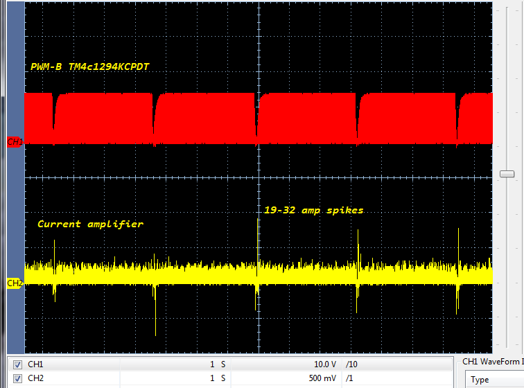
Have past posted similar question as to what can cause a reoccurring electrical disturbance on PWM between 1-5 seconds apart. Yet the 1/2 bridge output drives are very clean most of the time than suddenly 100-200ms crash of all PWM periods. How could I be so blind not to see this electrical storm as anything but disastrous.

It has more recently occurred to me that global synchronous updates may be out of sync during GPTM driven output intervals PWMENABLE register. Hence PWM outputs being enabled during generator counts being loaded may not be the best of all conditions. Oddly this frequent random storm does not crash the DC inverter but absolutely reeks havoc on hardware from the EMF spike/s that occur. Sort of like mowing your lawn where grass deepens having to push even harder to get through the rough. Upon exit there is a sudden moment when you accelerate then even out the self propelled speed. Since then purchased 42" deck rider mower but that's another yard story.

Anyway the GPTM configured OSHT has an interrupt handler function to control PWMENABLE and OSHT count is reloaded between 2 PWM periods inside the ADC interrupt handler.

Then there is another GPTM to capture edge times for the ADC interrupt, used to determine a new PWM edge for driving commutation via PWMENABLE, another NVIC interrupt.   

Perhaps PWM (over run) occurs during global synchronous updates, ADC interrupts indirectly control the outer commutation function loop via OSHT timeout.

The question is how to stop over run without adding to much complexity and or disrupting PWM commutation cycles? 

My first guess being to add a while Not loop into OSHT handler that drives commutation events, is that to evasive?

Has anyone ever seen this same random PWM electrical storm?

  • After longer Saturday review and hold off of further dutycycle updates during global synchronous updates made no difference. 

    What I now notice is slow decay seems the culprit. As duty cycle ramps up to 98% via roughly 10-15 PWM periods there is an current climax near the end of each build up in a repeating cycle. When climax occurs the current sensors go bonkers with high frequency high voltage transient response cycles util the storm is over. They get all excited then relax for a period after the storm. The current sensors detect up to -4v and pass zero crossing transient directly into the ADC, counter measures do exist.       

  • The low side switches period set near 100% seems to grow more saturated as duty cycle increases, PWM over run worsens at the end of each decay cycle. This leads to high current spikes, 25-30 amp peak surges. It is something in the PWM update and local dead band timing more likely that rudely disrupts high side NFET decay cycles.

    It's a bit alarming to see the PWM drives get randomly distorted as they do. Past chalked current climax events as being dV/dT related transient but this issue seems more like an over run of PWM drives near the end of slow decay cycles. The current climax event always occurs at the end of the low switches saturation ramp. That is the low side switches are not always 89-99% saturated as dead band cycles seem to play some part of the delay Off time.  The dead band generators (180ns) are not static register values they are switched on or off cycle by cycle as Wiki text related as being highly efficient.

  • It would seem from Table 1 and Figure 4 (link) the original SW never inverted PWM-B drives to active low state. Adding dynamic dead band switching control PWM-A/B mostly works. Yet TM4C1294 dead band generators input PWM-A, invert to make PWM-B drive signals. Table 1 row 1 infers PWM-B (2,4,6) are active low enable, PWM-A (1,3,5) are active high enable. Likely to account for complementary A/B drives with static dead band enabled. High efficiency hardware may set dead band dynamically as TI suggests in later NexFET and GAN analysis technical sheets.

    The TM4C1294 static dead band control example fails to demonstrate complementary PWM drive signals being properly configured. Why was the low side PWM-B drives never inverted active low enable prior to enabling dead band registers, per Table 1 row 1?   

    Adding slow decay seems to invite body diode shoot through if PWM-B drives are configured active high. According to Infineon this occurs any time the high side NFET turns on as the low side NFET freewheel diode has current flow, on any 1/2 bridge. Has the switch node shoot through been arrested via dynamic SW control of dead band generator seemingly yes.

    Has NFET freewheel diode Qrr/Trr been given ample recovery time prior to next PWM active switch event? Does the SW invert PWM-B drives, Yes but only during HW dead band control of any 1/2 bridge. Otherwise PMW-B drive is configured active high, Table 1 suggest active low enable.

    Seemingly PWM over run is likely to occur at the end of slow decay cycles (climax) if PWM-B drives are not configured active Low enabled. Seemingly the dead band example SW was configured incorrectly per Table 1 and leads to future issues that don't seem so obvious.

    http://www.ti.com/lit/an/spra289/spra289.pdf

  • Hi,

      Are you using the GPTM module or the PWM module for your PWM generation? On one hand, you talked about GPTM and on another you talked about PWMENABLE. The PWMENABLE is a register in the PWM module, not GPTM. 

      How do you know the PWM are out of sync? Do you have scope cap to show that? 

      What is OSHT? I can't find this abbreviation in the driverlib, datasheet and peripheral driver library user's guide. 

      If you are using the GPTM module to generate the PWM, did you set TnPLO and TnMRSU bits high? 


    If you are using the PWM module to generate the PWM then which sync method did you try? I will try the Globally synchronize method. 

    The counter in a PWM generator can be reset to zero by writing the PWM Time Base Sync
    (PWMSYNC) register and setting the SYNCn bit associated with the generator. Multiple PWM
    generators can be synchronized together by setting all necessary SYNCn bits in one access. For
    example, setting the SYNC0 and SYNC1 bits in the PWMSYNC register causes the counters in PWM
    generators 0 and 1 to reset together.


    Additional synchronization can occur between multiple PWM generators by updating register contents
    in one of the following three ways:


    ¡ Immediately. The write value has immediate effect, and the hardware reacts immediately.


    ¡ Locally Synchronized. The write value does not affect the logic until the counter reaches the
    value zero at the end of the PWM cycle. In this case, the effect of the write is deferred, providing
    a guaranteed defined behavior and preventing overly short or overly long output PWM pulses.


    ¡ Globally Synchronized. The write value does not affect the logic until two sequential events
    have occurred: (1) the Update mode for the generator function is programmed for global
    synchronization in the PWMnCTL register, and (2) the counter reaches zero at the end of the
    PWM cycle. In this case, the effect of the write is deferred until the end of the PWM cycle following
    the end of all updates. This mode allows multiple items in multiple PWM generators to be updated
    simultaneously without odd effects during the update; everything runs from the old values until
    a point at which they all run from the new values. The Update mode of the load and comparator
    match values can be individually configured in each PWM generator block. It typically makes
    sense to use the synchronous update mechanism across PWM generator blocks when the timers
    in those blocks are synchronized, although this is not required in order for this mechanism to
    function properly.

  • Hi Charles,

    This is PWM0 global sync with DB sync local. So PWM-A can not have the same duty as PWM-B when slow decay is active PWM-B.  The WA has been to only enable RED/FED for last on 1/2 bridge prior to new cycle. Otherwise there is no pass through DB when A inverts to makes B. The GPTM's OneShot (OSHT) control timing for commutation events via data PWM_ENABLE register. 

    I tested Table 1 row 1 with static RED/FED set after inverting PWM-B drives, was more like 1/2 bridge short condition. That is with local updates for PWM_ENABLE, past tried global and no sync neither one worked period.


  • Scope channels 10KSPS, 1k samples deep, no filtering. CH1 is All PWM-A/B phase drives and CH2 often peaks 25-30 amps @150vdc (not shown). The negative portion CH2 is most concerning. 


  • "Perfect Storm" (alleged) Greetings,

    Might some here find your scope presentation "Less than Perfect" and "Storm" reduced to Drizzle?

    Should not (some) Ground Rules prove in order?    (vendor agents too "nice" - too "PC bound" - to readily impose...)

    • This is primarily an MCU-centric forum - the issue you (uniquely) raise proves far more "BLDC Motor Control related."    Vendor agents are highly trained & skilled - yet such "deep dives" into, "Highly focused Application Specifics" is almost certain to "exceed their charter."   
    • Vendor provides (other) - more motor-related - forums.
    • It is unlikely that (any vendor's) MCU manual can fully/properly "anticipate & resolve" each/every user's "deep-dive" application requirement.   Such appears your expectation...

    To your post's specifics:

    • You report, "Capture of slow decay current buildup ramp" - yet neither "CH1 (Gate Driver) nor CH2 (Current Sensor)" reveal (any) form of buildup.   (to my group's perhaps "lesser trained eyes!")    Such "Building Ramp" should reveal as "Regularly Widening Gate Drive Pulses AND rising output from the Current Sensor" - should it not?   
    • You provide two signal captures - both "Foreign to your MCU!"   (The current sense waveform opens your report to (almost) unlimited "Application, Design & Implementation issues" - are you not seeking our "blind faith?")    While it is likely that the output from the gate-driver (CH1) closely follows (but for amplitude) that of the MCU - "professional diagnosticians always prefer the "real" MCU signals!"
    • Earlier posts w/in this thread (properly) noted "Half "H-Bridge" dead-band issues - yet no scope traces revealing those 'dead-band pairings' have arrived.   That's an oversight - is it not?
    • And - perhaps most importantly - "inadequate 'close-in' detail is presented "at/around" your (apparent) current surge!"    As that surge represents your (alleged) "storm" - even the terrific, "Detective Columbo" - would be hard pressed to "make a case" -w/so meager (i.e. essentially NO) evidence presented!    Multiple "key channels" displayed (far beyond the simple two presented) would tremendously heighten the "Recognition & Understanding" of "possible causative links!"     You place (very) high demands upon vendor agent helpers (even outsiders) - yet your instrumentation appears "vastly over-challenged" - that's (both) curious & less than helpful - & un-noted - until now...

    While we, "Feel your (ongoing) pain" - your method of,

    • Identifying & presenting the most central issues
    • Presenting those to the "most appropriate resource groups"

    may benefit from "more precise & targeted crafting."   It is (certainly) agreed that you have raised, "multiple points of interest."

    Many here, "Want you to succeed" - suggested are possible (even likely), "steps in that direction."

  • Hi,

      I don't know what to suggest and I have no knowledge of your system. You will need to figure out what is wrong yourself. Where you show the Perfect Storm coincides with some noise on your gate drive. See the noises inside the white circle. Why is that? I cannot help on this.

  • Hi Charles,

    Charles Tsai said:
    See the noises inside the white circle. Why is that? I cannot help on this.

    It is from CH2 riding on ground. Storm seems more like an synchronous update over run during PWMENABLE time frames. Oddly it can go very clean for some time then randomly have group of extremely high distortion pulses, CH2. Some of the SNR is scope aliasing or ground noise related but not all. 

    The only other possibility Systick interrupt handler is being interrupted by NVIC to clear his source. Systick is used to determine EMF edge times triggering an OSHT (oneshot) reload and to load PWM_ENABLE values to output on CH1. Should Systick ever get out of sync with PWM updates it could cause an over run during PWM synchronous updates, is another thought.

  • Gl said:
    The only other possibility Systick interrupt handler is being interrupted by NVIC to clear his source. Systick is used to determine EMF edge times triggering an OSHT reload and to load PWMENABLE values to output on CH1. Should Systick ever get out of sync with PWM updates it could cause an over run during PWM synchronous updates, is another thought.

    Systick is an exception that is of higher priority than the interrupts.

  • Hi Charles,

    Thank you for pointing this out and it had used GPTM1 periodic mode versus Systick. This SW has always had issues with dead band B inversion with slow decay being enabled. It seems several PWM design assumptions were made in this area of the SW.

    I have past looked at the PWM generator and assumed comparators were producing complement PWM outputs, equal duty cycles. But it seems comparators follow datasheet Fig.23-5 verbatim, leading to dead band issues. Looking at debug registers below notice PWMB uses CMPB-D/U, again verbatim Fig.23-5.

    Seemingly Fig.23-5 gives an example of what not to do and leads to dead band issues with slow decay enabled at the same time. Does it work,  that's debatable since it can't have static enabled dead band and slow decay. And PWM-B is not passed out but inverted PWM-A by dead band generators, verbatim. It seems overlapping signals may lead to partial 1/2 bridge shoot through via NFET low side body diodes even with dynamic dead band cycles. The datasheet next example (Fig.23-6) shows dead band possible with overlapping signals Fig.23-5, is that prudent? Perhaps another approach is more prudent with fewer dead band harmonics? 

    Oddly other PWM generators produce complementary GEN-A/B outputs as default comparator actions.

    1. Should we change GENB comparator B actions to be A actions to produce complement outputs PWM-A/B?

    2. Why does the datasheet not suggest the most common PWM output mode and dead band use? 

    3 Why is there no table for several different comparator configurations? 


    Seemingly Fig.23-5 can not produce the wave forms shown below so why mislead the community it does?

  • The most common PWM generator configuration do not have overlapping signals shown in Fig. 23-5. They are complementary A/B and only proper configuration of the comparators can ever produce pattern below. There are NO CMP-B actions Fig.3-10, contrary to past unfounded helper claims. The older LM3S and newer TM4C data sheets seem to mislead all to use CMP-B, thus static dead band show below fails to work per Fig. 23-6. Who would be the wiser until mayhem causes the perfect storm.  

  • Tivaware PWMPulseWidthSet() forces CMPB output if PWM drive bit has Odd value, forcing PWM-A/B outputs to produce overlapping signals. Seemingly that defeats dead band register RED/FED being statically enabled, with slow decay periods. Dynamic dead band was enabled for last PWMENABLE register GENn bits and PWM-B was being lost in dead band anyway, working from the last synchronous update values. 

    Why does Tivaware force CMPB and not allow the user to select the comparator as datasheet text infers to be quiet possible? Seemingly someone has pushed the easy button and not produced a viable pulse width set function and complementary PWM signals can NOT be easily produce. This seems to explain why the dead band Tivaware example fails in my testing of it.

    The comparators (CMP-A/B) actions are NOT output drives (PWM-A/B) and whoever developed pwm.c module did not know the difference. Otherwise the entire module should pass/check CMP selection A/B action with the pulse width value being passed into call below, rather than forcing it based on the PWM bits. Again CMP-A/B actions are NOT the PWM A/B outputs (INCORRECTLY) illustrated Fig.32-1 Fig.23-2. Otherwise the PWM module would be in conflict with datasheet text and figures that show CMP-A/B actions are PWM clock related INPUT actions for the PWM-A/B outputs.   

    void
    PWMPulseWidthSet(uint32_t ui32Base, uint32_t ui32PWMOut,
                     uint32_t ui32Width)
    {
       //~~~~~~~~~~~~~~~!!!!
       // other things it does
    
        //
        // Write to the appropriate registers.
        //
        if(PWM_IS_OUTPUT_ODD(ui32PWMOut))
        {
            HWREG(ui32GenBase + PWM_O_X_CMPB) = ui32Reg;
        }
        else
        {
            HWREG(ui32GenBase + PWM_O_X_CMPA) = ui32Reg;
        }
    }


  • Storm (not so much) Greetings,

    In addition to your "miss" of "Systick avoiding issues brought on by (mere) interrupts" it appears that you've not noted the preamble text to Fig. 23-5 (bottom line) which states, "Signals BEFORE they have passed through the dead-band generator!"

    Indeed - as I (past) many times presented for you (here) that "overlap of PWM_A & PWM_B is EASILY produced when "dead-band" is not commanded nor enabled.    Any "mislead of the community" springs from (other) than Fig 23-5!   (some suggest that a mirrored reflection - better identifies such source...)

  • Gl said:
    Seemingly Fig.23-5 can not produce the wave forms shown below so why mislead the community it does?

    The figure 23-5 merely demonstrates how to generate symmetrical PWM. This figure is inside section 23.3.4 PWM Signal Generator. Just because the section 23.3.4 is right before 23.3.5 Dead-Band Generator does not mean that you use the example in Figure 23-5 to generate dead-band signals. 

  • cb1_mobile said:
    Any "mislead of the community" springs from (other) than Fig 23-5! 

    Like the complete incompetence of someone who should have known better wrote the entire PWM.C for comparator outputs passing through dead band.

  • Gl said:
    There are NO CMP-B actions Fig.3-10, contrary to past unfounded helper claims.

    You are referencing an entirely different PWM module from the C2000 MCU. Each module has its own way of operations. You are comparing apple and orange. 

  • Charles Tsai said:
    Just because the section 23.3.4 is right before 23.3.5 Dead-Band Generator does not mean that you use the example in Figure 23-5 to generate dead-band signals. 

    Your missing the point that Tivaware forces PWM-B to use CMP-B as if it were the PWM-B output. There are two paths shown but no elaboration on either inside the blocks. So anyone sees this as Tivaware designer did incorrectly forced CMP-B to use PWM-B based on the pin position in PWMENABLE.

    To produce complementary A/B outputs without any overlap requires CMP-A be selected for both PWM-A/B output actions. That can not be achieved when any odd pin (low) is being forced by pulse width set to use CMP-B.

  • Vendor's API is "most always" an excellent guide & model.    (NO API - from any source - is able to meet "ALL NEEDS of ALL USERS ... at ALL TIMES!")

    Your (long) appearance here HAS produced progress - much attributable to the API.   (even pwm.c!)

    Nothing (beyond skill/time/effort) prevents you from modifying "pwm.c" to your own requirements.   (wise to rename the file so it is not over-written by (pending) API upgrades ... appears "the dog" ate the promised March 2020 update!)

  • Charles Tsai said:
    You are referencing an entirely different PWM module from the C2000 MCU.

    We can not make any other type output waveform other than overlapping from Tivaware pulse width set function. Comparator A/B are tied to the PWM clock as count actions for PWM-A/B outputs, not the outputs themselves. The comparator outputs internally control either generator A/B output relative to the PWM time base actions shown in Fig.23-4. That way other types of DSP wave forms can be easily generated based on specific comparator actions. 

    The way Tivaware PWMPulseWidthSet() was written only an overlapping signal pair can ever be generated.

  • Rapidly declining "storm" greetings,

    Gl said:
    The way Tivaware PWMPulseWidthSet() was written only an overlapping signal pair can ever be generated.

    UNTRUE - (community ALERT!) again I've produced multiple Scope-Caps for you - in proof of this fact.

    When the dead-band is properly enabled - and configured (both front & back end) a CLEARLY "Non-Overlapping" signal pair are most certainly produced!

  • Gl said:
    Your missing the point that Tivaware forces PWM-B to use CMP-B as if it were the PWM-B output.

    Where in the datasheet that says to use COMP-B to generate dead-band? 

    As I mentioned the figure in 23-5 has no relevance to dead-band generation. If figure 23-5 is 10 pages away (with other sections in between) from section 23.3.5 then you would not have related them together. 

  • Many forgetful salutations! 

    cb1_mobile said:
    Your (long) appearance here HAS produced progress - much attributable to the API.   (even pwm.c!)

    So naive thinking this code was gospel, issue dates back to Stellaris pwm.c.  Was looking for vendor confirmation that PWMPulseWidthSet() is not telling the truth perhaps your answer needs further investigation. Talk about a learning curve anyone can do without.....

    Wozniak & wife seen on TV last week claims back from China with corona late January, the most truth I've heard of late. Was sick myself, other family members back in Feb. from unknown virus, remnants still hanging on.

    Glad to here your staying safe from this outrageous pandemic! 

  • Charles Tsai said:
    Where in the datasheet that says to use COMP-B to generate dead-band? 

    Tivaware forces it in the code posted above from these calls below.

                MAP_PWMPulseWidthSet(PWM0_BASE, PWM_OUT_2, ulWidthA);//CMP-A HS
                MAP_PWMPulseWidthSet(PWM0_BASE, PWM_OUT_3, ulWidthA);//CMP-B LS

  • "Clever/Thoughtful" better described greetings,    (via young/gifted staff...)

    Might you glance (over/around) your "claim of storm" and ACCEPT:    (CH1: PWM_A,  CH2: PWM_B - Dead-Band enabled via API - w/out issue!)

    Dreaded overlap [your claim] (somehow) appears "Not much in Evidence!"   (As the API's (most proper) assertion of dead-band (both front & back end) assures!)    

    I did this for you here 3-4 years back - pity that it must be "re-called" today!   (scope reveals date of capture - 2016!)   Unfortunately the date of your "agreement" remains unknown - might (that) be the sole - and REAL Storm?

    e2e.ti.com/.../1900414

  • Gl said:

    Tivaware forces it in the code posted above from these calls below.

    1
    2
    MAP_PWMPulseWidthSet(PWM0_BASE, PWM_OUT_2, ulWidthA);//CMP-A HS
    MAP_PWMPulseWidthSet(PWM0_BASE, PWM_OUT_3, ulWidthA);//CMP-B LS

    Who says the PWMPulseWidthSet will infer the CMP-B? By hardware, the PWM-B is the inverse of PWM-A with programmable delay when dead-band is enabled. 

  • Charles Tsai said:
    Where in the datasheet that says to use COMP-B to generate dead-band? 

    Right dead band generators drop PWM-B and use PWM-A inverted to form PWM-B. We want the action from CMP-A for both PWM-A/B outputs when dynamic dead band is not enabled for the pair of driven 1/2 bridges via PWMENABLE outputs. We don''t require dead band when driving NFETS only when they are switched off (RED/FED) are asserted. 

    I see your point as for how static dead band might appear. If it does not first or at all use GEN PWM-B to set the internal input state prior to PWM-A inversion. The dead band paragraph seems to suggest PWM-B is not entirely lost and what does lost mean exactly in electronic terms?

  • Charles Tsai said:
    Who says the PWMPulseWidthSet will infer the CMP-B? By hardware, the PWM-B is the inverse of PWM-A with programmable delay when dead-band is enabled. 

    The debug register show what Tivaware and code that came from TI was incorrect to force CMP-B actions to qualify PWM-B output. If it were correct then we could enable static dead band interleaved with slow decay cycles. Why is that not possible, the only answer is we don't need slow decay if the PWM generator duty cycle updates do not force PWM-B to use CMP-B.

    Seemingly over lapping signals versus complementary signals produce wildly different inverter power levels. Why does TI adopt both PWM-A/B complementary outputs via (CMP-A) in all it's DC power inverters as shown above? 

  • cb1_mobile said:
    I did this for you here 3-4 years back - pity that it must be "re-called" today! 

    The worst part being how is PWM-B going to get updates if dead band is statically enabled? Sort of the point posting how a storm randomly develops every few 100 PWM cycles. Storm of course with dynamic dead bands. Dynamic that PWM-B updates can still work with slow decay enabled below otherwise it's a dead horse.

    Seemingly it may not be necessary to use slow decay or have uneven duty cycles when PWM-B can use  CMP-A actions to qualify both PWM-A/B outputs. That was not possible to test in Tivaware calls below that force ODD pins to use much wider CMP-B action counts.  

  • CB1,

    As the update code above infers pass through dead band is a challenge for dead band cycles. 

    HWREG calls to use CMP-A for both PWM-A/B will produce complementary outputs on each 1/2 bridge. Have you ever tested such scenario?

    Seemingly this can produce same or more power without slow decay just from even duty cycles, PWM-A/B. Perhaps current amp outputs will have more of a sinewave attribute is one thought. Who cares what the PWM looks like if CMP-A develops the robust even power distribution both high/low switches. 

  • Gl said:
    /* GEN1 pulse width update */
    MAP_PWMPulseWidthSet(PWM0_BASE, PWM_OUT_2, ulWidthA);//HS
    MAP_PWMPulseWidthSet(PWM0_BASE, PWM_OUT_3,
                         (g_ulPWMClock - (g_sParameters.ucDeadTime - 1 ))); //LS
     
    /* GEN2 pulse width update */
    MAP_PWMPulseWidthSet(PWM0_BASE, PWM_OUT_4, ulWidthB);//HS
    MAP_PWMPulseWidthSet(PWM0_BASE, PWM_OUT_5,
                         (g_ulPWMClock - (g_sParameters.ucDeadTime - 1 ))); //LS
     
    /* GEN3 pulse width update */
    MAP_PWMPulseWidthSet(PWM0_BASE, PWM_OUT_6, ulWidthC);//HS
    MAP_PWMPulseWidthSet(PWM0_BASE, PWM_OUT_7,
                         (g_ulPWMClock - (g_sParameters.ucDeadTime - 1 ))); //LS

    I do not see you call PWMDeadBandEnable() in your code. It seems you are trying to generate the dead-band signals manually when you can allow the hardware to generate the dead-band for you based on the EVEN pins. 

  • Shift from "blame" (misleading MCU manual) to (further) investigative (i.e. productive) Greetings,

    Staff pleasantly surprised re: your willingness to (now) potentially explore "solutions" - rather than "throw bombs."

    Our group is now split into thirds (we have multiple BLDC Controller (& motor) shipments to get out) - yet we will make the (added) effort to (further) guide you (as we have done often - long into the past!)

    Focused, KISS-based, probing experimentation long ago enabled my gifted staff to "tease out" a "highly satisfactory" solution.   We've repeatedly "urged you" in that direction - yet "complaining trumped focused effort..."

    We designed & then implemented multiple "Half-Bridge pcbs" (as THERE is where the "dead-band" ACTION really lies) and our "intense, multi-channel data measures & captures" - led directly to our success.

    "Intuition - often guessing" - proves no substitute for systematic, properly (deeply) considered experimentation."   (Somehow - such disciplined effort - proves "Storm-Free!")

  • Charles Tsai said:
    I do not see you call PWMDeadBandEnable() in your code

    As the word static dead band implies fixed configuration and dynamic a toggled time managed enabling.

    I found two problems, PWMGenConfigure() forces CMPB actions and the other was PWMPeriodSet(), each forced overlapping center aligned A/B signals as if that was the only possible configuration. It is not.

    Charles Tsai said:
    It seems you are trying to generate the dead-band signals manually when you can allow the hardware to generate the dead-band for you based on the EVEN pins. 

    Right and as explained how can HW update periods on PWM-B with slow decay enabled and static dead band has lost B? We are using local dead band updates so slow decay can coexist with dynamic dead band and updates on B. If dead band was not dynamic enabled during PWMENABLE periods there would be full shoot through on each 1/2 bridge. 

    Behold - center aligned complementary outputs with matching update pulse width set.

        /* Configure PWM0 for center aligned complementary GENA/GENB drives */
        HWREG(PWM0_BASE + PWM_O_1_GENA) = (PWM_X_GENA_ACTCMPAU_ONE | PWM_X_GENA_ACTCMPAD_ZERO);
        HWREG(PWM0_BASE + PWM_O_1_GENB) = (PWM_X_GENB_ACTCMPAU_ZERO  | PWM_X_GENB_ACTCMPAD_ONE);
        HWREG(PWM0_BASE + PWM_O_2_GENA) = (PWM_X_GENA_ACTCMPAU_ONE | PWM_X_GENA_ACTCMPAD_ZERO);
        HWREG(PWM0_BASE + PWM_O_2_GENB) = (PWM_X_GENB_ACTCMPAU_ZERO  | PWM_X_GENB_ACTCMPAD_ONE);
        HWREG(PWM0_BASE + PWM_O_3_GENA) = (PWM_X_GENA_ACTCMPAU_ONE | PWM_X_GENA_ACTCMPAD_ZERO);
        HWREG(PWM0_BASE + PWM_O_3_GENB) = (PWM_X_GENB_ACTCMPAU_ZERO  | PWM_X_GENB_ACTCMPAD_ONE);


  • cb1_mobile said:
    Shift from "blame" (misleading MCU manual) to (further) investigative (i.e. productive) Greetings,

    One can partially learn from written text and or later self discovery on other TI complex systems. Solutions were many times stopped by forum rejections that no other possible configuration existed beyond Fig. 23-5, though asked how many times past.  It takes time to become wise and aware to even question code or the text as being the end of all ends.

    Other forum folks can now post configure GENS to produce center aligned Non overlapping complementary wave forms. Complements are especially useful for DCDC converters and the two Tivaware calls above noted can use a makeover. Not yet sure how it may eliminate slow decay, being a bit early to post these findings. Perhaps complements will reduce annoying wa wa wa noise of overlapping drive signals. That alone is worth 1000 tank yous!

  • Complementary outputs required PWM-A' (high) drives be inverted and reduction duty cycle divisors or DC supply under voltage rapidly occurs. Oddly static dead band works yet duty cycle updates work backwards. Otherwise complementary GENA'/B' outputs would seem to work without slow decay via period set CMPA. The SW as coded takes advantage of odd inverted duty cycles such that lower PWMnLOAD values produce higher dutycycle %. So current starts out high then reduces during initial open loop current ramp. Yet current is very strong without slow decay CMPB cycles, backwards duty control a mystery.  

    All that is a bit more than bargained for without ability of GENA/B output inversion prior to dead band generator inputs. It seems the mere fact of using CMPB creates an overlapping signal no matter load value. That was reason to configure complementary outputs but the dead band generators have a different idea about easily made possible.

    Back to CMPA/B slow decay mode, scope probes uncover a 400ms PWM-A' drive void occurs every 30 10-12 seconds in channel scan mode similar to first capture posted. 

    That much interruption to PWM updates seems application related in some way. Oddly delay don't crash commutation but does cause a storm as CMPA returns 390ms latter. 

  • Revisionist History Greetings,

    Gl said:
    Other forum folks can now post configure GENS to produce center aligned Non overlapping complementary wave forms.

    What NOW?   Do you mean like (this) - (easily) achieved & presented here (for you) 4 years earlier?     (bottom right of scope cap records date of capture...)


  • Reaching for (beyond) "Partial Learning" Greetings,

    Gl said:
    One can partially learn from written text and or later self discovery on other TI complex systems.

    As my group has LONG & directly suggested to you (as well as numerous clients) - "Systematic, Focused, Insightful Experimentation" appears extremely helpful - often profoundly expanding the "Critical NEW Learning Process" - unlikely to arrive in (broad/past) & less exactingly crafted (i.e. challenge-lite) environments!

    Staff believes their development of (a near Army) of fundamental "Half-Bridge" pcbs - in a wide variety of components & ratings - goes far (often furthest) to "Speed, Ease & Enhance" (real) Learning!   

    It is known that (many/most) develop motor controllers via the "Full Board Approach."   Our group has found that (both) overly/unnecessarily expensive & hugely inefficient!    It is clear that the bulk of the Controlled-Power, "ACTION takes place w/in the Half-Bridges" - thus they should be "independently implemented" and optimized for:

    • Speed & Ease of Probing
    • Multiple key measurement/monitoring "Attachment Points"
    • Quick & Eased (and SAFE) "correct way only" Plug-In to a, "Receiving mother-board"
    • Multiple board - Current & Power capabilities - yielded effective measurements spanning 20-120 Amps & 40-160V (V_Motor)
    • Up to SIX of these Half-Bridge pcbs may be "plugged-in" to the controlling mother board.   Our design "sweated the details" to insure that, "LIVE BOARD SWAPS" could be achieved (under full-speed, full-power operation) so that the most accurate comparative measurements (automated, btw) were achieved!    Such "Swaps" were managed Electronically - all boards remained fully connected (i.e. isolated unless active) and all "Swaps" were under full "Command & Control!"

    Boards were designed w/4 Oz. Copper, multiple thermal vias, & non-symmetric (power-rated)) banana jacks & cables enabling rapid insertion/removal.    (Key clients sought "test to destruction" capability...)

    Follows several of our past board designs - which vastly enhanced our discovery of "Real-World Operational Performance Factors."     And - especially - How "Performance Optimization Factors" could best be realized!    Should it be noted that alternative (vastly less insightful) "written text" readings prove "FAR Less EFFECTIVE!"

    Our lowest current Half-Bridge (cost down).   All boards followed this "Size/Connection Model" easing & speeding "Insertion, Replacement & Critically Sought" (A vs B vs C vs D vs E vs F) Dynamic, Comparative  Measurements...   Nowhere else achievable - under such,"Tightly Controlled, Equalized & Highly Repeatable Test Conditions!"

    Two of the Eight Half-Bridges we developed to accommodate currents spanning 20-120A.  (board on the right employs top-cabin "dual-side" cooling capability.   custom, top-side heat-sink not shown)

    bottom view - revealing the high current Gate Driver & massive (4 Oz.) copper layer

  • cb1_mobile said:
    What NOW?   Do you mean like (this) - (easily) achieved & presented here (for you) 4 years earlier? 

    Are those not overlapping waveforms you picture above? Complementary pairs have a distinctly aligned PWM-A/B edge profile as shown below. Also tested inverted CMP-A/B, UP/DN configurations versus inverting the output of high side drives. And millisecond gap (PWM-A/B drives) also captured via Tektronix scope occurs no matter what, yet with less frequent visits to the blue light lane.

    Oddly the debug GENn load values go very low at that time but XDS102 never seems to capture load value 0x0 as gap occurs. After finagling was able to get SW to switch off slow decay during acceleration so both CMP-A/B have equal pulse width values near 0x42. Oddly the PWM-B times widened to closely match PWM-A gap width but occur much less frequently and the gap is now seconds wide, current goes nuts.

    Seemingly the PWM generators are Stalling for unknown undocumented reasons from very low LOAD values <0x100. Generator stalling causes a later phase current storm like heat lightning viewed from a distance. Arresting generator count stalling is the goal to achieve by any means. Oddly the A/B generator period load value 0x5dc drop rapidly <0x3C, lower rotor speeds. One can only imagine how snarky current behaves at higher speeds when PWM generators randomly stall counts. BTW nice PCB work such high hair raising currents.


  • Slow decay PWM-B load value 0x7 locks in and CMP-B gap narrows, CMP-A gap remains the same width. When both PWM-A/B have equal load values (0x3c) without slow decay locking CMP-B  the gap gets seconds wide and current gets extremely periodic, spiking occurs. The answer long saught after is at hand,  seemingly HW configuration of PWM module is to blame and undocumented errata occurs!  

  • I tested forcing pwmA/B low during zero INT update but it made no difference to stop generator stalling events. Condensed datasheet of GEN/A-B control actions below. The PWMn control registers set the comparator zero/load actions, they are now 0x0 do nothing. Forcing PWM-A/B low during load did not stop generator stalling. I'm not sure how forcing them to any state can or will arrest generator count stalling.   

    Register 44: PWM0 Generator A Control (PWM0GENA), offset 0x060
    Register 45: PWM1 Generator A Control (PWM1GENA), offset 0x0A0
    Register 46: PWM2 Generator A Control (PWM2GENA), offset 0x0E0
    Register 47: PWM3 Generator A Control (PWM3GENA), offset 0x120

    Register 48: PWM0 Generator B Control (PWM0GENB), offset 0x064
    Register 49: PWM1 Generator B Control (PWM1GENB), offset 0x0A4
    Register 50: PWM2 Generator B Control (PWM2GENB), offset 0x0E4
    Register 51: PWM3 Generator B Control (PWM3GENB), offset 0x124

    These registers control the generation of the pwmA/B signal based on the load and zero output pulses from the counter, as well as the compare A and compare B pulses from the comparators (PWM0GENA/B controls the PWM generator 0 block, and so on). When the counter is running in
    Count-Down mode, only four of these events occur; when running in Count-Up/Down mode, all six occur. These events provide great flexibility in the positioning and duty cycle of the resulting PWM signal.  

    The PWM0GENA/B registers controls generation of the pwm0A/B signal; PWM1GENA/B, the pwm1A/B signal; PWM2GENA/B, the pwm2A/B signals; and PWM3GENA/B, the pwm3A/B signals. If a zero or load event coincides with a compare A or compare B event, the zero or load action is taken and the compare A or compare B action is ignored. If a compare A event coincides with a compare B event, the compare A action is taken and the compare B action is ignored.

    Action for Comparator A/B UP / Down
    This field specifies the action to be taken when the counter matches
    comparator A while counting down.
    Value Description
    0x0 Do nothing.
    0x1 Invert pwmA/B.
    0x2 Drive pwmA/B Low.
    0x3 Drive pwmA/B High.

  • Unable and/or Unwilling to "Master the Basics" Greetings,

    Gl said:
    Are those not overlapping waveforms you picture above?

    No - as (most here) will agree - the scope cap reveals a properly formed, Complementary Pair of PWM Outputs - set w/equal value dead-band - imposed upon (both) leading & trailing edge of PWM_A.   (CH1)

    The time/effort required to provide such a scope-cap for you was in response to your,  "Other forum folks can now post configure GENS to produce center aligned Non overlapping complementary wave forms."

    Both PWM Outputs shown drive an appropriate Gate Driver (positive logic - inputs active high) which in turn provides proper signal level to a pair of "Power N-FETs" - which excite one phase of a BLDC Motor.   And which deliver BLDC Motor Currents approaching 100 Amps - while (never) evidencing deadly, "Overlap" - certain to cause Power-FET "Shoot-Through!"

    For any "overlap" to be noted - both PWM Outputs must be active (i.e. High) at the same time.    Clearly any such (destructive) overlap is "Not at All" visible here.   It is unknown as to "Why you believe (any) overlap has occurred!"    And proves likely to "cast doubt upon" other of your findings & beliefs...

    As you (continue) to fully reject, "Experimentation" (as a learning aid) - and appear challenged by "overlap recognition" - your note of "Storm Clouds overtaking the horizon" are expected to (LONG) continue.

    Staff/I "wish you well" - yet your quest to be "right" far exceeds your acceptance of, "Better Means & Methods!"

  • cb1_mobile said:
    No - as (most here) will agree - the scope cap reveals a properly formed, Complementary Pair of PWM Outputs - set w/equal value dead-band - imposed upon (both) leading & trailing edge of PWM_A.   (CH1)

    The context we were speaking of generators CMP-A/B producing non overlapping signals, NOT with dead band enabled. I was unaware you had included dead band in your 2nd capture of the overlap signals discussion, Fig. 23-5.  Adding dead band does not produce overlapping signal pairs, it only delays the generator signal passed into it from PWM-A. I was specifically indicating how overlapping versus non overlapping signals are created and generated, not with dead band.

    Please try to find solutions for blank PWM periods posted several times, destroy any production via this MCU class. Why do you think the current amplifiers perform so badly with this MCU, the proof is in the capture below. It seems you are more interested in combat than answering the questions posted, if not my appologies. Yet this vendor should try to answer why voids are appearing PWM-A'/B' when SW writes into PWM_ENABLE register.

    The odd errata discovered via PWM_ENABLE output is clear evidence of sequential truncating PWM-A generator outputs. Oddly if we set no sync on PWM_ENALE register a few pulses show up in the blank void areas of only PWM-B'. 

        MAP_PWMOutputUpdateMode(PWM0_BASE, (PWM_OUT_2_BIT | PWM_OUT_3_BIT | PWM_OUT_4_BIT |
                                            PWM_OUT_5_BIT | PWM_OUT_6_BIT | PWM_OUT_7_BIT),
    							PWM_OUTPUT_MODE_NO_SYNC);//PWM_OUTPUT_MODE_SYNC_LOCAL
    

  • Obviously it is not proper to have current surges mid power cycles on any phase. Note CH2 current sensor amplifier transient response upon several ADC channels. Thus a highly distorted representation of incorrect sample values will thwart any attempt to achieve precision results. Yet the faster PWM beats voids the less obvious amplifier SNR becomes as low pass SW filters tweak out obscure random surges.

    Thus the perfect storm this MCU sets sail, unless.....

  • Gl said:
    Thus the perfect storm this MCU sets sail

    Somehow the movie line, "Mad Captain - Rudderless Ship" sails into frame.   (the over-written "BP" remains visible upon ship's stern...)

    Our "repeated guidance" to, "Design & Implement Focused & Properly Measured Experimentation" (as we highly detailed for you) runs strongly counter to your erroneous claim, "more interested in combat than answering the questions posted."    Our posts targeted "direct statements by you" (which were "quoted") [as evidence] & were clearly "OFF Mark" and demanding challenge for the "Protection of others!"  

  • Seemingly you had misinterpreted my point was an attempt to establish NON overlapping PWM-A'/B' drives, to alter the issue base line. Complementary signal pairs can never be accomplished via CMP-A/B, as depicted Fig.23-5. That method clearly develops overlapping signals via triangle PWM clock source with CMP-B leading CMP-A on up counts.

    If the PWM clock source was square wave Fig.23-5, different story altogether. CMP-B has no option on the way up or down but to lead and lag signals generated via CMP-A. However when we only configure CMP-A the story has a different plot and even more so for CMP-B alone. The lower complementary values CMP-B will push current earlier sweeps of duty cycle values and equally shared switching currents low/high NFETS.

    The odd part being PWM_ENABLE register bits never stop toggling for 300-600ms shown scope captures. Yet the GPIO high skew rate PWM configured MCU pins do have clear voids with no pulse train. The PWM_ENABLE signals out to the MCU pins are being interrupted during that time. This is not so easily detected at higher duty cycles as the void gap nearly closes but the current transients remain to reek havoc on ADC samples. Who'd be the wiser to think voids in PWM could cause current surges, seemingly not even CB1. 

    How to get values PWM_ENABLE register bits out to MCU pins with out blanking voids seems the gotcha challenge. 

  • Gl said:
    Yet the GPIO high skew rate PWM configured MCU pins do have clear voids with no pulse train.

    Can you create a program which runs on a standard launchpad which demonstrates this problem?

    If so, that would allow others to investigate a potential software issue or device errata.

  • I would should FE have no explanation to how or why the PWM_ENABLE would void GPIO states out to MCU pins.I've checked for shared GPIO pin overlaps or interrupt conflicts, there are none. What ever gates generator counts PWM-A/B into PWM_ENABLE register  suspect cause of signal voids. Oddly if the output mode is changed to _No_Sync the low PWM-B get a few pulses inside the voids. 

    We can only view enable state bits PWM_ENABLE register, not the actual transfer of PWM-A/B generator signals into or out to package pins. Some thing is blanking the counter outputs to PWM_ENABLE, but not the enable state. From the description below it seems the generators are being synchronized during the PWM voids on GPIO pins. That is not the same as enabling bits PWMCTL for global synchronous updates. Tested enabling global after each PWM_ENABLE register write and nothing changed.  Writes to PMW_ENABLE register occur 50µs intervals @20kHz.  My gut tells me the generators are re-synchronizing but the PWMSYNC status bits are to fast to capture via XDS102 ICDI on launch pad.

    Register 3: PWM Output Enable (PWMENABLE), offset 0x008

    This register provides a master control of which generated pwmA' and pwmB' signals are output to the MnPWMn pins. By disabling a PWM output, the generation process can continue (for example, when the time bases are synchronized) without driving PWM signals to the pins. When bits in this register are set, the corresponding pwmA' or pwmB' signal is passed through to the output stage. When bits are clear, the pwmA' or pwmB' signal is replaced by a zero value which is also passed to the output stage. The PWMINVERT register controls the output stage, so if the corresponding bit is set in that register, the value seen on the MnPWMn signal is inverted from what is configured by the bits in this register. Updates to the bits in this register can be immediate or locally or globally synchronized to the next synchronous update as controlled by the ENUPDn fields in the PWMENUPD register.

  • Insuring PWM synchronization SW monitor REG4 did not stop the void issue. That still is not evidence PWM generators are not auto ReSync at higher speed than can be detected by XDS102 ICDI or CCS debug. 

    	/* Synchronize the PWM generators time bases.  */
    	HWREG(PWM0_BASE + PWM_O_SYNC) =
    			(PWM_GEN_0_BIT | PWM_GEN_1_BIT | PWM_GEN_2_BIT | PWM_GEN_3_BIT);
    	/* Do nothing else until all bits REG4 cleared */
    	while(!HWREG(PWM0_BASE + PWM_O_SYNC) ==
    			~(PWM_GEN_0_BIT | PWM_GEN_1_BIT | PWM_GEN_2_BIT | PWM_GEN_3_BIT))
    	{
    	}

    Up to today testing was on EK-TM4C1294XL launch pad. Oddly custom PCB (TM4C1294KCPDT) MCU has a lot more frequent PWM interruptions (CH1). A recent thought occurred, scope horizontal time base set to Scan or Roll may not trigger for frequency >20kHz, even scope samples 100KSPS, 10KS deep.

    Repeating voids (current spikes) CH2 may not actually be zero counts (CH1), rather consist of very high PWM frequency >100KHz. The only way to know might require an attached frequency counter scope triggered during scan or roll modes. 

    Notice the repeating interval are seconds apart on the KCPDT and >10 seconds on the NCPDT.