This thread has been locked.

If you have a related question, please click the "Ask a related question" button in the top right corner. The newly created question will be automatically linked to this question.

TM4C123FH6PM: Tvia MCU Vs ADC Interface

Part Number: TM4C123FH6PM
Other Parts Discussed in Thread: THS1206, TMS320C6201,

Hello 

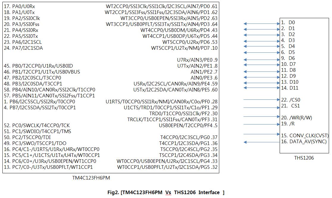
Q1> How do I interface with Tvia MCU(TM4C123FH6PMI7) and Ti ADC(THS1206)?

       - I received THS1206EVM source code from ADC Forum, but I don't know.

         https://e2e.ti.com/support/data-converters/f/73/p/911632/3390319#3390319

       - The attached image below is the interface information between the desired devices.

Best Regards,
Jame, Shin

  • Hi Jame,

      In my opinion, I think the THS1206 ADC converter is not a suitable choice. I will suggest you look into ADC converter with the same capability as THS1206 but provides a serial interface (e.g. SPI, I2C, UART) to the MCU. If you are going to use the TM4C123 to interface to the THS1206, you will need to bit-bang using GPIO mode which is doable but much more complex. Unlike the TMS320 processors, the TM4C123 does not have an external peripheral interface. 

  • Hello Charles,

    The ADC sample rate is low for more than 4 ADC serial interfaces (e.g. SPI, I2C, UART) required. ( e.g. 1MSPS/1ch, 250KSPS/4ch).

    4Ch ADC Module, 54Mhz BW, 12bit, Parallel interface to apply high sample rate (6MSPS / 1Ch, 1.5MSPS / 4Ch).

    The source code of the address linked in the previous post seems to depend on the MSP430 MCU.

    By the way, the source code looks simple and seems to drive a parallel interface by using the GPIO port.

    Q2> Even if the MCU device TM4C123 is changed to TM4C129, is it the same complex as using a bit-bang in GPIO mode?

    Best Regards,
    Jame, Shin

  • Hi Jame,

      I didn't see the link you provided last time. Ok, it looks like it is manageable to use the bit-bang method on GPIO to access the ADC. I still think it is more complex than having a serial interface. If you can't find a suitable converter with the serial interface then I guess you just need to go ahead with the bit-bang. Since you already have the source code for MSP430 then I don't think it will be too difficult to migrate to TM4C123. You just need to find the available GIO ports on the TM4C123 device to do the bit-bang. 

    Jame shin said:
    Q2> Even if the MCU device TM4C123 is changed to TM4C129, is it the same complex as using a bit-bang in GPIO mode?

    I don't think it will be more difficult or easier when you change to TM4C129. You will be using the same TivaWare after all for both devices. 

  • Hello Charles,

    I am worried about using DSPs (①TMS320C30/31/33 or ②TMS320C54x or ③ TMS320C6201) instead of Tiva MCU for THS1206 interface.

    However, I am afraid that I have not studied DSPs.

    Because I had time and effort to study Tiva MCU.

    Q3> Which is a good way? (This is a silly question. !!)

    regards,

    Jame, Shin

  • Hi Jame,

      I don't think you should change to the TMS320 processors. I will suggest you just port the code you have from MSP to TM4C. 

  • Hello Charles,

    In the previous post Fig2, I’m thinking about how to provide THS1206 (15pin, CONV_CLK) device clock.

    Clock Spec THS1206(15pin, CONV_CLK)

         Input CON_CLK frequency (min) 0.1Mhz (max) 6Mhz

         - Clock high, CONV_CLKH (min) 80ns (typ) 83ns (max)5000ns

         - Clock low, CONV_CLKL (min) 80ns (typ) 83ns (max)5000ns

    Q4> Is it possible to output PWM 6Mhz from TM4C123 device MCU?

            Please let me know if there is a good way.

    Best Regards,
    Jame, Shin

  • Hi Jame,

      Please refer to the possible System Clock frequency in table 5-4 and 5-5 in your device datasheet. Your PWM frequency will be divisible by the System Clock. You can come close to 6Mhz but not exactly. Why are you using PWM to generate clock? I thought you are going to use bit-bang method. If you use PWM to generate the clock to the THS1206, then how do you synchronize your data (if you use bit-bang for the data) to the PWM?

  • Hello Charles,

    If I look at the MSP source code provided in the ADC forum, there is no GPIO setting and I am not sure. 

    So, looking at the timing diagram of THS1206, I am thinking one by one.

    Also, I read and studied the bit band of TM4C data sheet before.

    I understood that the bit operation control in the existing GPIO port changes the bit value directly from RMW method to SRAM address setting.

    Of course, using the bit-banding you mentioned, I'm trying to create control and data signals for the THS1206 device on the MCU.

    Previous post, See Fig2. [TM4C123FH6PM Vs THS1206 Interface]

     -Control signal : /CS0, CS1, /WR , /R , CONV_CLK(CVST),  DATA_AV(SYNC)

     -Data signal    :  D[11 : 0]


    Charles_Q1> Why are you using PWM to generate clock?

    Jame_ A1> I thought it was difficult to generate 0.1Mhz ~ 6Mhz clock by utilizing Bit-Band.

                   So I thought it would be easy to use PWM output signal.

                  CONV_CLK describes the clock required for the number of analog input channels in the TH1206 data sheet.

                     1Ch ADC  / 1 CONV_CLK

                     2Ch ADC  / 2 CONV_CLK

                     3Ch ADC  / 3 CONV_CLK

                     4Ch ADC  / 4 CONV_CLK

                   i.e) Converted analog input signal to ADC with CONV_CLK(CVST) and saved as 16x12bit FIFO.

                        And, DATA_AV(SYNC) signal is output high to read data in FIFO.

                        Then TM4C MCU is interrupted by high detection of DATA_AV(SYNC) signal and reads data in TH1206 FIFO.

    Charles_Q2> …., how do you synchronize your data (if you use bit-bang for the data) to the PWM ?

    Jame_ A2> THS1206 The data sheet is described as controlling the clock timing on the device.

                    I am not sure about synchronizing the clock.

         Conversion Modes (in TH1206 Datasheet)

             The conversion can be performed in two different conversion modes.

             In the single conversion mode, the conversion is initiated by an external signal (CONVST). .

             An internal oscillator controls the conversion time. .

             In the continuous conversion mode, an external clock signal is applied to the clock input (CONV_CLK). .

             A new conversion is started with every falling edge of the applied clock signal.

    Please advise how to do it.

    Best Regards,
    Jame, Shin

  • Hi,

      I really don't know what else to suggest you. My best advice for you is to convert the sample code you obtained from MSP and convert it to TIVA. I'm not sure what difficulty you have to convert from MSP to Tiva. Although they are two different devices but the concept of using bit-bang in either device should be similar. Let's say in the MSP they you Port A, B to perform the bit bang and you need to use Port E and F in Tiva, I just think it is doable to convert to Tiva. 

     If you want to use PWM to generate a continuous clock then I think it is fine. You just need to experiment with it. I don't know TH1206 at all. Perhaps there is no need to do synchronization between the CONV_CLK and reading the data from the FIFO. Sorry, if I mislead you on that in my last reply.

  • Hello Charles,

    Your answers have been advanced and helpful with a lot of hints and thoughts.

    Thank you. Also, please be interested in threads in the future.

    regards,

    Jame,Shin