This thread has been locked.

If you have a related question, please click the "Ask a related question" button in the top right corner. The newly created question will be automatically linked to this question.

CCS/TM4C123GH6PM: read spi using pwm as clock

Part Number: TM4C123GH6PM
Other Parts Discussed in Thread: ADS8326, ADS8319

Tool/software: Code Composer Studio

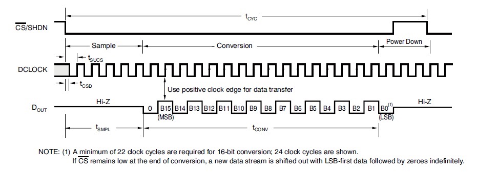
I have a question about SPI timing. I would like to read a 16 bit ADC (ADS8326) at 250 ksps using a TM4C123 microcontroller running at 80 MHz.  The timing diagram for the ADC is attached.

I need to drive CS low and have the MISO pin ignore 5 clock cycles before collecting data (attached timing diagram).  To do this, I think I need to set up the clock and CS pins as pwm signals and trigger the SSIDataGet command off of the CS timer.  My question; how do I set it up to read at the correct time?  I would like to set a flag in the ISR that is recognized in the main while(1) loop.  Do I need to introduce a delay, as in the text below, or will the MISO wait for the ADC output to drive the pin LOW?

if(readFlag == true){
SysCtlDelay(readDelay);
SSIDataGet(SSI0_BASE, &dataPoint);
}  

Thanks for your help.

Jack


  • Jack Summers11 said:
    To do this, I think I need to set up the clock and CS pins as pwm signals and trigger the SSIDataGet command off of the CS timer.

    When the TM4C123 SPI module is the SPI master, then the SPI module needs to generate the clock by calling SSIDataPut(). I.e. don't see that triggering SSIDataGet() off of the CS timer would work.

    Jack Summers11 said:
     I would like to read a 16 bit ADC (ADS8326) at 250 ksps using a TM4C123 microcontroller running at 80 MHz.

    Is 250 ksps a sustained capture of a sequence of back-to-back samples?

    250 ksps means a DCLOCK frequency of 6 MHz with a repeating cycle of:

    1. CS high for 2 clocks - ADS8326 "Power Down"
    2. CS low for 22 clocks for one sample - 6 clocks for ADS8326 "Sample" and 16 clocks for ADS8326 "Conversion"

    With the TM4C system clock at 80 MHz, then as the SPI module clock can only be an integer division of the system clock then it won't be possible to set the SPI clock to 6 MHz.

    Also, since it is a falling edge on CS which starts the ADS8326 Sample then how the CS is generated will impact any "jitter" on the timing of consecutive samples is started.

    How often do you need to make the ADS8326 collect a sample?

  • Hi Chester,

    I take your point about 6 MHz not being achievable with the 80 MHz master clock.

    The ADC reads have to synch up with outputs from a CCD array that is optimized to run at 250 kHz.  My guess is that the CCD performance will not be terribly affected if I slow the clock down.  If I slow the SPI clock to 4 MHz and use the 24 clocks, then my read frequency will be 167 kHz, which I can probably live with.

    The problem of synching the reads with the CCD output remains.  The CCD currently outputs a voltage every 4 us (frequency can be changed) until it outputs data for each of its ~4600 pixels.  If I slow the CCD clock down, I will still need to collect samples every 6 us.

    That gets us back to the SPI timing.  I believe that I need 22 clocks while CS is low and tivaware is only set up for 4, 8 or 16.  As I understand it, I will need to call SSIDataPut at least twice.  Then I need to toggle CS, which will also add time.  I guess I can just throw away all of the non-data bits, but the timing will be totally screwed up.

    I guess I could go with a faster ADC.  The ADS8319 says 500 ksps, but at first glance it looks like the timing  will still be an issue.

    Any suggestions?

    Thanks,
    Jack

  • Jack Summers11 said:
    I take your point about 6 MHz not being achievable with the 80 MHz master clock.

    Using a TM4C129 device, with a 120 MHz master clock, you should then be able to achieve a 6 MHz SPI clock. However the ADS8326 datasheet gives the fDCLOCK max of 6 MHz with a 5V supply, and a max of 4.8 MHz with a 2.7V supply.

    What VDD is your ADS8326 operating at?

    Jack Summers11 said:
    I believe that I need 22 clocks while CS is low and tivaware is only set up for 4, 8 or 16.

    The ui32DataWidth argument of SSIConfigSetExpClk() can take a value from 4 to 16 inclusive.

    If ui32DataWidth was set to 11 then two calls to SSIDataPut() and SSIDataGet() would result in 22 bits.

    Jack Summers11 said:
    Then I need to toggle CS, which will also add time. 

    If CS is toggled as a GPIO then that will add time, and potentially add variation on how the samples from the CCD are taken across all the pixels.

    Do interrupts or any background processing need to occur while the ~4600 pixels are being collected from the CCD?

  • I did not know you could set the data width like that. Thanks, that is good to know.

    I have a 501(c)(3) that builds low cost scientific instruments for education. This project is for a usb powered spectrometer.  I was planning to run the ADC off the same 3.3 volt source as the microcontroller, but I could take up to 5 volts from usb.

    Regarding your question about interrupts & background processing:  There is an interrupt that occurs periodically.  The period (the CCD integration time) is specified by the end user and is typically on the order of 2-20 ms.  When this interrupt occurs, all the clocks are reset to keep everything in sync.  The only processing that needs to occur is to put the data into an array.  Data from the array are output to the user after the acquisition phase is finished.

    I was thinking that the CS could be toggled as a pwm, which could be kept in sync with the rest of the instrument.  I could also call the SSIDataPut and SSIDataGet off the pwm interrupt.

    Changing the microcontroller right now would be a big step in the prototyping process.  I have several copies of a working prototype that reads the CCD using the 12 bit ADC internal to the TM4C123.  My current goal is to build a breakout board that plugs onto headers on the existing prototype and improves the resolution.   The current prototype has breakout header positions that allow access to the pins I need.  If I go through prototyping the ADC board with the current microcontroller board and find I need more speed down the line, I can do that later.  Of course the final product should have the ADC and microcontroller on a single board, but using what I already have saves a lot of time spent with the microscope and soldering iron.

    Thanks again,

    Jack

  • Jack Summers11 said:
    I was thinking that the CS could be toggled as a pwm, which could be kept in sync with the rest of the instrument.  I could also call the SSIDataPut and SSIDataGet off the pwm interrupt.

    I think the PWM timing for generating the CS would have to allow for the time to service the interrupt to ensure the SSIDataPut triggers the generation of DCLOCK to perform the sample and conversion, and if other interrupts require servicing could corrupt the capture by making the CS out of sync with the SPI clock.

    How important is for the operation of the spectrometer to take CCD samples at a fixed interval, minimizing timing 'jitter'?

  • I do not know how important the timing jitter would be, but my guess is that it would not matter as long as the CS stayed in sync with the CCD clock and as long as there was enough time for data transfer to complete before the CCD advances to the next pixel.

    I believe the CCD has an array of capacitors that each hold a charge and the array is read sequentially. My guess is that the charge is stable for more than the 4 us interval that the data sheet specifies.  If I were to collect data at 125 kHz, then I would have 8 us to sample the voltage and transfer the data.  Running the SCK at 4 MHz would give 6 us of data acquisition and transfer and leave 2 us to soak up any jitter.

    If the voltage is fairly constant over that period, then jitter between when CS toggles and the SCK starts would not be that important.  The important thing would be for the CS to stay in sync with the CCD clock to be sure we do not miss any pixels or count any pixels twice.

    In theory, I could collect data at 250 kHz and 125 kHz using my current prototype and compare the data sets to see if there is loss of the late acquired signal. The problem there is that I would have to disassemble the instrument to change the firmware and I am unlikely to get the optics aligned exactly the same way twice.

    Thanks again for your help.  I think that I have enough of a handle on it now that I can play around with the firmware and observe how the code executes on the scope.  I am also going to look at the data sheets for faster ADCs and see if going that direction would be a better option for me.  For once, I have actually tried to anticipate problems before ordering pcbs and hardware (I may be learning)!

    I will keep this thread open for a day or two in case you have any comments then I will credit you with resolving my issue.  If you are interested, you can  see photos of earlier spectrometer prototypes at smokymtsci.com/spectroscopy

    Best regards,

    Jack

  • Jack Summers11 said:
    The important thing would be for the CS to stay in sync with the CCD clock to be sure we do not miss any pixels or count any pixels twice.

    OK, having looked at the TCD1304DG CCD detector datasheet I now understand that the CS for the ADS8319 needs to be kept in step with the clock for the CCD, so that the ADC samples each pixel as it is clocked out of the linear CCD array.