Hi team,
we are using TMS570LC4357 processor for our project. Our requirement is to configure the SPI in master mode and establish the communication with the slave connected via available Chip Selects. For this operation, we are using the SPI3 configured in master mode, which is used in 4-mode, where along with SPI3CLK, SPI3SOMI, SPI3MISO we are using SPI3_CS0.
Here, the peripheral clock i.e. VCLK1 is configured as 90MHz and the SPICLK is 400Khz. and SPI3 is used in 8 bit char length with clock mode and clock polarity enabled. (Used FMT0 register).
As provided in the reference example we initialize the SPI3 and tried to establish the communication with the slave.
We configured all required pins as attached reference code.
We are observing that there is no data getting transmitted or received as chip select is not getting asserted or de-asserted. We have tried to probe the SPI pins but there was no data observed and chip select was continuously high.
We have also verified pin_mux configuration. We are stuck at this point and not able to proceed or get any breakthrough.
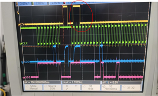
As a work a round, we tried to configure SPI3CS0 as GIO and tried asserting /de-asserting manually for transmission and reception.
During this we received the wrong data which we are suspecting that others external signals are disturbing the required chip select.
Attached is the waveform when chip select is configured as GIO. (Highlighted the false de-asserting of chip select)
Regards
Aporva
#include "HL_spi.h"
#include "HL_sys_vim.h"
/* USER CODE BEGIN (1) */
/* USER CODE END */

/** @struct g_spiPacket
*   @brief globals
*
*/
static volatile struct g_spiPacket
{
    spiDAT1_t g_spiDataFormat;
    uint32  tx_length;
    uint32  rx_length;
    uint16  * txdata_ptr;
    uint16  * rxdata_ptr;
    SpiDataStatus_t tx_data_status;
    SpiDataStatus_t rx_data_status;
} g_spiPacket_t[5U];

/** @fn void spiInit(void)
*   @brief Initializes the SPI Driver
*
*   This function initializes the SPI module.
*/
/* SourceId : SPI_SourceId_001 */
/* DesignId : SPI_DesignId_001 */
/* Requirements : HL_CONQ_SPI_SR7, HL_CONQ_SPI_SR8 */
void spiInit(void)
{
/* USER CODE BEGIN (2) */
/* USER CODE END */


    /** @b initialize @b SPI3 */

    /** bring SPI out of reset */
    spiREG3->GCR0 = 0U;
    spiREG3->GCR0 = 1U;

    /** SPI3 master mode and clock configuration */
    spiREG3->GCR1 = (spiREG3->GCR1 & 0xFFFFFFFCU) | ((uint32)((uint32)1U << 1U)  /* CLOKMOD */
                  | 1U);  /* MASTER */

    /** SPI3 enable pin configuration */
    spiREG3->INT0 = (spiREG3->INT0 & 0xFEFFFFFFU) | (uint32)((uint32)0U << 24U);  /* ENABLE HIGHZ */

    /** - Delays */
    spiREG3->DELAY = (uint32)((uint32)0U << 24U)  /* C2TDELAY */
                   | (uint32)((uint32)0U << 16U)  /* T2CDELAY */
                   | (uint32)((uint32)0U << 8U)   /* T2EDELAY */
                   | (uint32)((uint32)0U << 0U);  /* C2EDELAY */

    /** - Data Format 0 */
    spiREG3->FMT0 = (uint32)((uint32)0U << 24U)  /* wdelay */
                  | (uint32)((uint32)0U << 23U)  /* parity Polarity */
                  | (uint32)((uint32)0U << 22U)  /* parity enable */
                  | (uint32)((uint32)0U << 21U)  /* wait on enable */
                  | (uint32)((uint32)0U << 20U)  /* shift direction */
                  | (uint32)((uint32)1U << 17U)  /* clock polarity */
                  | (uint32)((uint32)1U << 16U)  /* clock phase */
                  | (uint32)((uint32)224U << 8U) /* baudrate prescale */
                  | (uint32)((uint32)8U << 0U);  /* data word length */

    /** - Data Format 1 */
    spiREG3->FMT1 = (uint32)((uint32)0U << 24U)  /* wdelay */
                  | (uint32)((uint32)0U << 23U)  /* parity Polarity */
                  | (uint32)((uint32)0U << 22U)  /* parity enable */
                  | (uint32)((uint32)0U << 21U)  /* wait on enable */
                  | (uint32)((uint32)0U << 20U)  /* shift direction */
                  | (uint32)((uint32)0U << 17U)  /* clock polarity */
                  | (uint32)((uint32)0U << 16U)  /* clock phase */
                  | (uint32)((uint32)89U << 8U) /* baudrate prescale */
                  | (uint32)((uint32)16U << 0U);  /* data word length */

    /** - Data Format 2 */
    spiREG3->FMT2 = (uint32)((uint32)0U << 24U)  /* wdelay */
                  | (uint32)((uint32)0U << 23U)  /* parity Polarity */
                  | (uint32)((uint32)0U << 22U)  /* parity enable */
                  | (uint32)((uint32)0U << 21U)  /* wait on enable */
                  | (uint32)((uint32)0U << 20U)  /* shift direction */
                  | (uint32)((uint32)0U << 17U)  /* clock polarity */
                  | (uint32)((uint32)0U << 16U)  /* clock phase */
                  | (uint32)((uint32)89U << 8U) /* baudrate prescale */
                  | (uint32)((uint32)16U << 0U);  /* data word length */

    /** - Data Format 3 */
    spiREG3->FMT3 = (uint32)((uint32)0U << 24U)  /* wdelay */
                  | (uint32)((uint32)0U << 23U)  /* parity Polarity */
                  | (uint32)((uint32)0U << 22U)  /* parity enable */
                  | (uint32)((uint32)0U << 21U)  /* wait on enable */
                  | (uint32)((uint32)0U << 20U)  /* shift direction */
                  | (uint32)((uint32)0U << 17U)  /* clock polarity */
                  | (uint32)((uint32)0U << 16U)  /* clock phase */
                  | (uint32)((uint32)89U << 8U) /* baudrate prescale */
                  | (uint32)((uint32)16U << 0U);  /* data word length */

    /** - set interrupt levels */
    spiREG3->LVL = (uint32)((uint32)0U << 9U)  /* TXINT */
                 | (uint32)((uint32)0U << 8U)  /* RXINT */
                 | (uint32)((uint32)0U << 6U)  /* OVRNINT */
                 | (uint32)((uint32)0U << 4U)  /* BITERR */
                 | (uint32)((uint32)0U << 3U)  /* DESYNC */
                 | (uint32)((uint32)0U << 2U)  /* PARERR */
                 | (uint32)((uint32)0U << 1U) /* TIMEOUT */
                 | (uint32)((uint32)0U << 0U);  /* DLENERR */

    /** - clear any pending interrupts */
    spiREG3->FLG |= 0xFFFFU;

    /** - enable interrupts */
    spiREG3->INT0 = (spiREG3->INT0 & 0xFFFF0000U)
                  | (uint32)((uint32)0U << 9U)  /* TXINT */
                  | (uint32)((uint32)0U << 8U)  /* RXINT */
                  | (uint32)((uint32)0U << 6U)  /* OVRNINT */
                  | (uint32)((uint32)0U << 4U)  /* BITERR */
                  | (uint32)((uint32)0U << 3U)  /* DESYNC */
                  | (uint32)((uint32)0U << 2U)  /* PARERR */
                  | (uint32)((uint32)0U << 1U) /* TIMEOUT */
                  | (uint32)((uint32)0U << 0U);  /* DLENERR */

    /** @b initialize @b SPI3 @b Port */

    /** - SPI3 Port output values */
    spiREG3->PC3 =    (uint32)((uint32)1U << 0U)  /* SCS[0] */
                    | (uint32)((uint32)1U << 1U)  /* SCS[1] */
                    | (uint32)((uint32)1U << 2U)  /* SCS[2] */
                    | (uint32)((uint32)1U << 3U)  /* SCS[3] */
                    | (uint32)((uint32)1U << 4U)  /* SCS[4] */
                    | (uint32)((uint32)1U << 5U)  /* SCS[5] */
                    | (uint32)((uint32)0U << 8U)  /* ENA */
                    | (uint32)((uint32)0U << 9U)  /* CLK */
                    | (uint32)((uint32)0U << 10U)  /* SIMO */
                    | (uint32)((uint32)0U << 11U); /* SOMI */

    /** - SPI3 Port direction */
    spiREG3->PC1  =   (uint32)((uint32)1U << 0U)  /* SCS[0] */
                    | (uint32)((uint32)1U << 1U)  /* SCS[1] */
                    | (uint32)((uint32)1U << 2U)  /* SCS[2] */
                    | (uint32)((uint32)1U << 3U)  /* SCS[3] */
                    | (uint32)((uint32)1U << 4U)  /* SCS[4] */
                    | (uint32)((uint32)1U << 5U)  /* SCS[5] */
                    | (uint32)((uint32)0U << 8U)  /* ENA */
                    | (uint32)((uint32)1U << 9U)  /* CLK */
                    | (uint32)((uint32)1U << 10U)  /* SIMO */
                    | (uint32)((uint32)0U << 11U); /* SOMI */

    /** - SPI3 Port open drain enable */
    spiREG3->PC6  =   (uint32)((uint32)0U << 0U)  /* SCS[0] */
                    | (uint32)((uint32)0U << 1U)  /* SCS[1] */
                    | (uint32)((uint32)0U << 2U)  /* SCS[2] */
                    | (uint32)((uint32)0U << 3U)  /* SCS[3] */
                    | (uint32)((uint32)0U << 4U)  /* SCS[4] */
                    | (uint32)((uint32)0U << 5U)  /* SCS[5] */
                    | (uint32)((uint32)0U << 8U)  /* ENA */
                    | (uint32)((uint32)0U << 9U)  /* CLK */
                    | (uint32)((uint32)0U << 10U)  /* SIMO */
                    | (uint32)((uint32)0U << 11U); /* SOMI */

    /** - SPI3 Port pullup / pulldown selection */
    spiREG3->PC8  =   (uint32)((uint32)1U << 0U)  /* SCS[0] */
                    | (uint32)((uint32)1U << 1U)  /* SCS[1] */
                    | (uint32)((uint32)1U << 2U)  /* SCS[2] */
                    | (uint32)((uint32)1U << 3U)  /* SCS[3] */
                    | (uint32)((uint32)1U << 4U)  /* SCS[4] */
                    | (uint32)((uint32)1U << 5U)  /* SCS[5] */
                    | (uint32)((uint32)1U << 8U)  /* ENA */
                    | (uint32)((uint32)1U << 9U)  /* CLK */
                    | (uint32)((uint32)1U << 10U)  /* SIMO */
                    | (uint32)((uint32)1U << 11U); /* SOMI */

    /** - SPI3 Port pullup / pulldown enable*/
    spiREG3->PC7  =   (uint32)((uint32)0U << 0U)  /* SCS[0] */
                    | (uint32)((uint32)0U << 1U)  /* SCS[1] */
                    | (uint32)((uint32)0U << 2U)  /* SCS[2] */
                    | (uint32)((uint32)0U << 3U)  /* SCS[3] */
                    | (uint32)((uint32)0U << 4U)  /* SCS[4] */
                    | (uint32)((uint32)0U << 5U)  /* SCS[5] */
                    | (uint32)((uint32)1U << 8U)  /* ENA */
                    | (uint32)((uint32)0U << 9U)  /* CLK */
                    | (uint32)((uint32)0U << 10U)  /* SIMO */
                    | (uint32)((uint32)0U << 11U); /* SOMI */

    /* SPI3 set all pins to functional */
    spiREG3->PC0  =   (uint32)((uint32)1U << 0U)  /* SCS[0] */
                    | (uint32)((uint32)0U << 1U)  /* SCS[1] */
                    | (uint32)((uint32)0U << 2U)  /* SCS[2] */
                    | (uint32)((uint32)0U << 3U)  /* SCS[3] */
                    | (uint32)((uint32)0U << 4U)  /* SCS[4] */
                    | (uint32)((uint32)0U << 5U)  /* SCS[5] */
                    | (uint32)((uint32)0U << 8U)  /* ENA */
                    | (uint32)((uint32)1U << 9U)  /* CLK */
                    | (uint32)((uint32)1U << 10U)  /* SIMO */
                    | (uint32)((uint32)1U << 11U); /* SOMI */

    /** - Initialize TX and RX data buffer Status */
    g_spiPacket_t[2U].tx_data_status  = SPI_READY;
    g_spiPacket_t[2U].rx_data_status  = SPI_READY;

    /** - Finally start SPI3 */
    spiREG3->GCR1 = (spiREG3->GCR1 & 0xFEFFFFFFU) | 0x01000000U;


/* USER CODE BEGIN (3) */
/* USER CODE END */
}


/** @fn void spiSetFunctional(spiBASE_t *spi, uint32 port)
*   @brief Change functional behavior of pins at runtime.
*   @param[in] spi   - Spi module base address
*   @param[in] port  - Value to write to PC0 register
*
*   Change the value of the PC0 register at runtime, this allows to
*   dynamically change the functionality of the SPI pins between functional
*   and GIO mode.
*/
/* SourceId : SPI_SourceId_002 */
/* DesignId : SPI_DesignId_002 */
/* Requirements : HL_CONQ_SPI_SR9 */
void spiSetFunctional(spiBASE_t *spi, uint32 port)
{
/* USER CODE BEGIN (4) */
/* USER CODE END */

    spi->PC0 = port;

/* USER CODE BEGIN (5) */
/* USER CODE END */
}


/** @fn uint32 spiReceiveData(spiBASE_t *spi, spiDAT1_t *dataconfig_t, uint32 blocksize, uint16 * destbuff)
*   @brief Receives Data using polling method
*   @param[in] spi           - Spi module base address
*   @param[in] dataconfig_t    - Spi DAT1 register configuration
*   @param[in] blocksize    - number of data
*   @param[in] destbuff        - Pointer to the destination data (16 bit).
*
*   @return flag register value.
*
*   This function transmits blocksize number of data from source buffer using polling method.
*/
/* SourceId : SPI_SourceId_003 */
/* DesignId : SPI_DesignId_007 */
/* Requirements : HL_CONQ_SPI_SR14 */
uint32 spiReceiveData(spiBASE_t *spi, spiDAT1_t *dataconfig_t, uint32 blocksize, uint16 * destbuff)
{
/* USER CODE BEGIN (6) */
/* USER CODE END */
    uint32 Chip_Select_Hold = (dataconfig_t->CS_HOLD) ? 0x10000000U : 0U;
    uint32 WDelay = (dataconfig_t->WDEL) ? 0x04000000U : 0U;
    SPIDATAFMT_t DataFormat = dataconfig_t->DFSEL;
    uint8 ChipSelect = dataconfig_t->CSNR;

    while(blocksize != 0U)
    {
        if((spi->FLG & 0x000000FFU) !=0U)
        {
          break;
        }
        if(blocksize == 1U)
        {
           Chip_Select_Hold = 0U;
        }

        /*SAFETYMCUSW 51 S MR:12.3 <APPROVED> "Needs shifting for 32-bit value" */
        spi->DAT1 = ((uint32)DataFormat << 24U) |
                    ((uint32)ChipSelect << 16U) |
                    (WDelay)            |
                    (Chip_Select_Hold)  |
                    (0x00000000U);
        /*SAFETYMCUSW 28 D MR:NA <APPROVED> "Hardware status bit read check" */
        while((spi->FLG & 0x00000100U) != 0x00000100U)
        {
        } /* Wait */
        /*SAFETYMCUSW 45 D MR:21.1 <APPROVED> "Valid non NULL input parameters are only allowed in this driver" */
        *destbuff = (uint16)spi->BUF;
        /*SAFETYMCUSW 567 S MR:17.1,17.4 <APPROVED> "Pointer increment needed" */
        destbuff++;
        blocksize--;
    }

/* USER CODE BEGIN (7) */
/* USER CODE END */

    return (spi->FLG & 0xFFU);
}


/** @fn uint32 spiGetData(spiBASE_t *spi, spiDAT1_t *dataconfig_t, uint32 blocksize, uint16 * destbuff)
*   @brief Receives Data using interrupt method
*   @param[in] spi           - Spi module base address
*   @param[in] dataconfig_t    - Spi DAT1 register configuration
*   @param[in] blocksize    - number of data
*   @param[in] destbuff        - Pointer to the destination data (16 bit).
*
*   @return flag register value.
*
*   This function transmits blocksize number of data from source buffer using interrupt method.
*/
/* SourceId : SPI_SourceId_004 */
/* DesignId : SPI_DesignId_008 */
/* Requirements : HL_CONQ_SPI_SR15 */
void spiGetData(spiBASE_t *spi, spiDAT1_t *dataconfig_t, uint32 blocksize, uint16 * destbuff)
{
     uint32 index = (spi == spiREG1) ? 0U :((spi==spiREG2) ? 1U : ((spi==spiREG3) ? 2U:((spi==spiREG4) ? 3U:4U)));

/* USER CODE BEGIN (8) */
/* USER CODE END */

     g_spiPacket_t[index].rx_length = blocksize;
     g_spiPacket_t[index].rxdata_ptr   = destbuff;
     g_spiPacket_t[index].g_spiDataFormat = *dataconfig_t;
     g_spiPacket_t[index].rx_data_status = SPI_PENDING;

     spi->INT0 |= 0x0100U;

/* USER CODE BEGIN (9) */
/* USER CODE END */
}


/** @fn uint32 spiTransmitData(spiBASE_t *spi, spiDAT1_t *dataconfig_t, uint32 blocksize, uint16 * srcbuff)
*   @brief Transmits Data using polling method
*   @param[in] spi           - Spi module base address
*   @param[in] dataconfig_t    - Spi DAT1 register configuration
*   @param[in] blocksize    - number of data
*   @param[in] srcbuff        - Pointer to the source data ( 16 bit).
*
*   @return flag register value.
*
*   This function transmits blocksize number of data from source buffer using polling method.
*/
/* SourceId : SPI_SourceId_005 */
/* DesignId : SPI_DesignId_005 */
/* Requirements : HL_CONQ_SPI_SR12 */
uint32 spiTransmitData(spiBASE_t *spi, spiDAT1_t *dataconfig_t, uint32 blocksize, uint16 * srcbuff)
{
    volatile uint32 SpiBuf;
    uint16 Tx_Data;
    uint32 Chip_Select_Hold = (dataconfig_t->CS_HOLD) ? 0x10000000U : 0U;
    uint32 WDelay = (dataconfig_t->WDEL) ? 0x04000000U : 0U;
    SPIDATAFMT_t DataFormat = dataconfig_t->DFSEL;
    uint8 ChipSelect = dataconfig_t->CSNR;

/* USER CODE BEGIN (10) */
/* USER CODE END */
    while(blocksize != 0U)
    {
        if((spi->FLG & 0x000000FFU) !=0U)
        {
           break;
        }

        if(blocksize == 1U)
        {
           Chip_Select_Hold = 0U;
        }
        /*SAFETYMCUSW 45 D MR:21.1 <APPROVED> "Valid non NULL input parameters are only allowed in this driver" */
        Tx_Data = *srcbuff;

        spi->DAT1 =  ((uint32)DataFormat << 24U) |
                     ((uint32)ChipSelect << 16U) |
                     (WDelay)           |
                     (Chip_Select_Hold) |
                     (uint32)Tx_Data;
        /*SAFETYMCUSW 567 S MR:17.1,17.4 <APPROVED> "Pointer increment needed" */
        srcbuff++;
        /*SAFETYMCUSW 28 D MR:NA <APPROVED> "Hardware status bit read check" */
        while((spi->FLG & 0x00000100U) != 0x00000100U)
        {
        } /* Wait */
        SpiBuf = spi->BUF;

        blocksize--;
    }

/* USER CODE BEGIN (11) */
/* USER CODE END */

    return (spi->FLG & 0xFFU);
}


/** @fn void spiSendData(spiBASE_t *spi, spiDAT1_t *dataconfig_t, uint32 blocksize, uint16 * srcbuff)
*   @brief Transmits Data using interrupt method
*   @param[in] spi           - Spi module base address
*   @param[in] dataconfig_t    - Spi DAT1 register configuration
*   @param[in] blocksize    - number of data
*   @param[in] srcbuff        - Pointer to the source data ( 16 bit).
*
*   @return flag register value.
*
*   This function transmits blocksize number of data from source buffer using interrupt method.
*/
/* SourceId : SPI_SourceId_006 */
/* DesignId : SPI_DesignId_006 */
/* Requirements : HL_CONQ_SPI_SR13 */
void spiSendData(spiBASE_t *spi, spiDAT1_t *dataconfig_t, uint32 blocksize, uint16 * srcbuff)
{
        uint32 index = (spi == spiREG1) ? 0U :((spi==spiREG2) ? 1U : ((spi==spiREG3) ? 2U:((spi==spiREG4) ? 3U:4U)));

/* USER CODE BEGIN (12) */
/* USER CODE END */

     g_spiPacket_t[index].tx_length = blocksize;
     g_spiPacket_t[index].txdata_ptr   = srcbuff;
     g_spiPacket_t[index].g_spiDataFormat = *dataconfig_t;
     g_spiPacket_t[index].tx_data_status = SPI_PENDING;

     spi->INT0 |= 0x0200U;

/* USER CODE BEGIN (13) */
/* USER CODE END */
}


/** @fn uint32 spiTransmitAndReceiveData(spiBASE_t *spi, spiDAT1_t *dataconfig_t, uint32 blocksize, uint16 * srcbuff, uint16 * destbuff)
*   @brief Transmits and Receive Data using polling method
*   @param[in] spi           - Spi module base address
*   @param[in] dataconfig_t    - Spi DAT1 register configuration
*   @param[in] blocksize    - number of data
*   @param[in] srcbuff        - Pointer to the source data ( 16 bit).
*   @param[in] destbuff        - Pointer to the destination data ( 16 bit).
*
*   @return flag register value.
*
*   This function transmits and receives blocksize number of data from source buffer using polling method.
*/
/* SourceId : SPI_SourceId_007 */
/* DesignId : SPI_DesignId_009 */
/* Requirements : HL_CONQ_SPI_SR16 */
uint32 spiTransmitAndReceiveData(spiBASE_t *spi, spiDAT1_t *dataconfig_t, uint32 blocksize, uint16 * srcbuff, uint16 * destbuff)
{
    uint16 Tx_Data;
    uint32 Chip_Select_Hold = (dataconfig_t->CS_HOLD) ? 0x10000000U : 0U;
    uint32 WDelay = (dataconfig_t->WDEL) ? 0x04000000U : 0U;
    SPIDATAFMT_t DataFormat = dataconfig_t->DFSEL;
    uint8 ChipSelect = dataconfig_t->CSNR;

/* USER CODE BEGIN (14) */
/* USER CODE END */
    while(blocksize != 0U)
    {
        if((spi->FLG & 0x000000FFU) != 0U)
        {
           break;
        }

        if(blocksize == 1U)
        {
           Chip_Select_Hold = 0U;
        }
        /*SAFETYMCUSW 45 D MR:21.1 <APPROVED> "Valid non NULL input parameters are only allowed in this driver" */
        Tx_Data = *srcbuff;

        spi->DAT1 =((uint32)DataFormat << 24U) |
                   ((uint32)ChipSelect << 16U) |
                   (WDelay)           |
                   (Chip_Select_Hold) |
                   (uint32)Tx_Data;
        /*SAFETYMCUSW 567 S MR:17.1,17.4 <APPROVED> "Pointer increment needed" */
        srcbuff++;
        /*SAFETYMCUSW 28 D MR:NA <APPROVED> "Hardware status bit read check" */
        while((spi->FLG & 0x00000100U) != 0x00000100U)
        {
        } /* Wait */
        /*SAFETYMCUSW 45 D MR:21.1 <APPROVED> "Valid non NULL input parameters are only allowed in this driver" */
        *destbuff = (uint16)spi->BUF;
        /*SAFETYMCUSW 567 S MR:17.1,17.4 <APPROVED> "Pointer increment needed" */
        destbuff++;

        blocksize--;
    }

/* USER CODE BEGIN (15) */
/* USER CODE END */

    return (spi->FLG & 0xFFU);
}

/* USER CODE BEGIN (16) */
/* USER CODE END */

/** @fn void spiSendAndGetData(spiBASE_t *spi, spiDAT1_t *dataconfig_t, uint32 blocksize, uint16 * srcbuff, uint16 * destbuff)
*   @brief Initiate SPI Transmits and receive Data using Interrupt mode.
*   @param[in] spi           - Spi module base address
*   @param[in] dataconfig_t    - Spi DAT1 register configuration
*   @param[in] blocksize    - number of data
*   @param[in] srcbuff        - Pointer to the source data ( 16 bit).
*   @param[in] destbuff        - Pointer to the destination data ( 16 bit).
*
*   Initiate SPI Transmits and receive Data using Interrupt mode..
*/
/* SourceId : SPI_SourceId_008 */
/* DesignId : SPI_DesignId_010 */
/* Requirements : HL_CONQ_SPI_SR17 */
void spiSendAndGetData(spiBASE_t *spi, spiDAT1_t *dataconfig_t, uint32 blocksize, uint16 * srcbuff, uint16 * destbuff)
{

/* USER CODE BEGIN (17) */
/* USER CODE END */

    uint32 index = (spi == spiREG1) ? 0U :((spi==spiREG2) ? 1U : ((spi==spiREG3) ? 2U:((spi==spiREG4) ? 3U:4U)));

    g_spiPacket_t[index].tx_length       = blocksize;
    g_spiPacket_t[index].rx_length       = blocksize;
    g_spiPacket_t[index].txdata_ptr      = srcbuff;
    g_spiPacket_t[index].rxdata_ptr      = destbuff;
    g_spiPacket_t[index].g_spiDataFormat = *dataconfig_t;
    g_spiPacket_t[index].tx_data_status  = SPI_PENDING;
    g_spiPacket_t[index].rx_data_status  = SPI_PENDING;

    spi->INT0 |= 0x0300U;

/* USER CODE BEGIN (18) */
/* USER CODE END */
}

/** @fn SpiDataStatus_t SpiTxStatus(spiBASE_t *spi)
*   @brief Get the status of the SPI Transmit data block.
*   @param[in] spi           - Spi module base address
*
*   @return Spi Transmit block data status.
*
*   Get the status of the SPI Transmit data block.
*/
/* SourceId : SPI_SourceId_009 */
/* DesignId : SPI_DesignId_013 */
/* Requirements : HL_CONQ_SPI_SR20 */
SpiDataStatus_t SpiTxStatus(spiBASE_t *spi)
{

/* USER CODE BEGIN (19) */
/* USER CODE END */

    uint32 index = (spi == spiREG1) ? 0U :((spi==spiREG2) ? 1U : ((spi==spiREG3) ? 2U:((spi==spiREG4) ? 3U:4U)));
    return(g_spiPacket_t[index].tx_data_status);
}

/* USER CODE BEGIN (20) */
/* USER CODE END */

/** @fn SpiDataStatus_t SpiRxStatus(spiBASE_t *spi)
*   @brief Get the status of the SPI Receive data block.
*   @param[in] spi           - Spi module base address
*
*   @return Spi Receive block data status.
*
*   Get the status of the SPI Receive data block.
*/
/* SourceId : SPI_SourceId_010 */
/* DesignId : SPI_DesignId_014 */
/* Requirements : HL_CONQ_SPI_SR21 */
SpiDataStatus_t SpiRxStatus(spiBASE_t *spi)
{

/* USER CODE BEGIN (21) */
/* USER CODE END */

    uint32 index = (spi == spiREG1) ? 0U :((spi==spiREG2) ? 1U : ((spi==spiREG3) ? 2U:((spi==spiREG4) ? 3U:4U)));
    return(g_spiPacket_t[index].rx_data_status);
}

/* USER CODE BEGIN (22) */
/* USER CODE END */

/** @fn void spiEnableLoopback(spiBASE_t *spi, loopBackType_t Loopbacktype)
*   @brief Enable Loopback mode for self test
*   @param[in] spi        - spi module base address
*   @param[in] Loopbacktype  - Digital or Analog
*
*   This function enables the Loopback mode for self test.
*/
/* SourceId : SPI_SourceId_011 */
/* DesignId : SPI_DesignId_011 */
/* Requirements : HL_CONQ_SPI_SR18 */
void spiEnableLoopback(spiBASE_t *spi, loopBackType_t Loopbacktype)
{
/* USER CODE BEGIN (23) */
/* USER CODE END */

    /* Clear Loopback incase enabled already */
    spi->IOLPKTSTCR = 0U;

    /* Enable Loopback either in Analog or Digital Mode */
    spi->IOLPKTSTCR = (uint32)0x00000A00U
                    | (uint32)((uint32)Loopbacktype << 1U);

/* USER CODE BEGIN (24) */
/* USER CODE END */
}

/* USER CODE BEGIN (25) */
/* USER CODE END */

/** @fn void spiDisableLoopback(spiBASE_t *spi)
*   @brief Enable Loopback mode for self test
*   @param[in] spi        - spi module base address
*
*   This function disable the Loopback mode.
*/
/* SourceId : SPI_SourceId_012 */
/* DesignId : SPI_DesignId_012 */
/* Requirements : HL_CONQ_SPI_SR19 */
void spiDisableLoopback(spiBASE_t *spi)
{
/* USER CODE BEGIN (26) */
/* USER CODE END */

    /* Disable Loopback Mode */
    spi->IOLPKTSTCR = 0x00000500U;

/* USER CODE BEGIN (27) */
/* USER CODE END */
}

/* USER CODE BEGIN (28) */
/* USER CODE END */

/** @fn spiEnableNotification(spiBASE_t *spi, uint32 flags)
*   @brief Enable interrupts
*   @param[in] spi   - spi module base address
*   @param[in] flags - Interrupts to be enabled, can be ored value of:
*/
/* SourceId : SPI_SourceId_013 */
/* DesignId : SPI_DesignId_003 */
/* Requirements : HL_CONQ_SPI_SR10 */
void spiEnableNotification(spiBASE_t *spi, uint32 flags)
{
/* USER CODE BEGIN (29) */
/* USER CODE END */

    spi->INT0 = (spi->INT0 & 0xFFFF0000U) | flags;

/* USER CODE BEGIN (30) */
/* USER CODE END */
}

/* USER CODE BEGIN (31) */
/* USER CODE END */

/** @fn spiDisableNotification(spiBASE_t *spi, uint32 flags)
*   @brief Enable interrupts
*   @param[in] spi   - spi module base address
*   @param[in] flags - Interrupts to be enabled, can be ored value of:
*/
/* SourceId : SPI_SourceId_014 */
/* DesignId : SPI_DesignId_004 */
/* Requirements : HL_CONQ_SPI_SR11 */
void spiDisableNotification(spiBASE_t *spi, uint32 flags)
{
/* USER CODE BEGIN (32) */
/* USER CODE END */

    spi->INT0 = (spi->INT0 & (~(flags)));

/* USER CODE BEGIN (33) */
/* USER CODE END */
}


/** @fn void spi3GetConfigValue(spi_config_reg_t *config_reg, config_value_type_t type)
*   @brief Get the initial or current values of the configuration registers
*
*    @param[in] *config_reg: pointer to the struct to which the initial or current
*                           value of the configuration registers need to be stored
*    @param[in] type:     whether initial or current value of the configuration registers need to be stored
*                        - InitialValue: initial value of the configuration registers will be stored
*                                       in the struct pointed by config_reg
*                        - CurrentValue: initial value of the configuration registers will be stored
*                                       in the struct pointed by config_reg
*
*   This function will copy the initial or current value (depending on the parameter 'type')
*   of the configuration registers to the struct pointed by config_reg
*
*/
/* SourceId : SPI_SourceId_017 */
/* DesignId : SPI_DesignId_015 */
/* Requirements : HL_CONQ_SPI_SR26 */
void spi3GetConfigValue(spi_config_reg_t *config_reg, config_value_type_t type)
{
    if (type == InitialValue)
    {
        config_reg->CONFIG_GCR1  = SPI3_GCR1_CONFIGVALUE;
        config_reg->CONFIG_INT0  = SPI3_INT0_CONFIGVALUE;
        config_reg->CONFIG_LVL   = SPI3_LVL_CONFIGVALUE;
        config_reg->CONFIG_PC0   = SPI3_PC0_CONFIGVALUE;
        config_reg->CONFIG_PC1   = SPI3_PC1_CONFIGVALUE;
        config_reg->CONFIG_PC6   = SPI3_PC6_CONFIGVALUE;
        config_reg->CONFIG_PC7   = SPI3_PC7_CONFIGVALUE;
        config_reg->CONFIG_PC8   = SPI3_PC8_CONFIGVALUE;
        config_reg->CONFIG_DELAY = SPI3_DELAY_CONFIGVALUE;
        config_reg->CONFIG_FMT0  = SPI3_FMT0_CONFIGVALUE;
        config_reg->CONFIG_FMT1  = SPI3_FMT1_CONFIGVALUE;
        config_reg->CONFIG_FMT2  = SPI3_FMT2_CONFIGVALUE;
        config_reg->CONFIG_FMT3  = SPI3_FMT3_CONFIGVALUE;
    }
    else
    {
    /*SAFETYMCUSW 134 S MR:12.2 <APPROVED> "LDRA Tool issue" */
        config_reg->CONFIG_GCR1  = spiREG3->GCR1;
        config_reg->CONFIG_INT0  = spiREG3->INT0;
        config_reg->CONFIG_LVL   = spiREG3->LVL;
        config_reg->CONFIG_PC0   = spiREG3->PC0;
        config_reg->CONFIG_PC1   = spiREG3->PC1;
        config_reg->CONFIG_PC6   = spiREG3->PC6;
        config_reg->CONFIG_PC7   = spiREG3->PC7;
        config_reg->CONFIG_PC8   = spiREG3->PC8;
        config_reg->CONFIG_DELAY = spiREG3->DELAY ;
        config_reg->CONFIG_FMT0  = spiREG3->FMT0;
        config_reg->CONFIG_FMT1  = spiREG3->FMT1;
        config_reg->CONFIG_FMT2  = spiREG3->FMT2;
        config_reg->CONFIG_FMT3  = spiREG3->FMT3;
    }
}