Other Parts Discussed in Thread: TM4C123GH6PZ
Hello Experts,
I understand, that U1 and U2 on the abovementioned Launchpad are both the same IC. Namely: TM4C123G-H6PMI, while U1 is the chip that is connected to the pin header, the LED, etc and U2 is used only as the programmer and debugger.
1. is it true, that, used as it is here, U2 functions basically as a debug probe, like for example, a XDS110 JTAG Debug Probe would?
2. when I plug in USB to the debug port and do an ICDI Firmware Update with the LM Flash Programmer, this is the process that programs U2 to be a programmer/debugger, right?
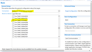
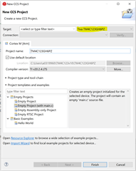
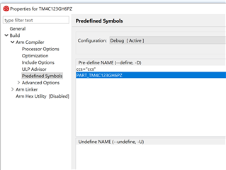
I want to use the TM4C123GH6PZT7 for my embedded solution. (the 100 pin version of the chip, since I need more gpio)
The idea is to do it in the same way as it is done on the launchpad, just a different U1. That means the TM4C123G-H6PZT7 as U1 and the -H6PMI as U2. The rest stays pretty much the same.
Let's assume I wire everything up as was done on the launchpad (PA0 - PA5 of U2 to the corresponding pins of U1 and PD4/PD5 of U2 to the USB interface) and use factory new chips:
3. can I just plug USB in, do an ICDI Firmware Update with the LM Flash Programmer and have U2 work as the programmer/debugger? Or do I need to make an additional step with factory new chips?
4. will I be able to programm/debug my U1 (TM4C123G-H6PZT7) in the same way I am with the launchpad?
Thank you very much.
Regards
Lucas