This thread has been locked.

If you have a related question, please click the "Ask a related question" button in the top right corner. The newly created question will be automatically linked to this question.

Interfacing 32x16 Dot Matrix Display to TM4c1294ncpdt (SPI interface)

Other Parts Discussed in Thread: TM4C1294NCPDT

Hi,

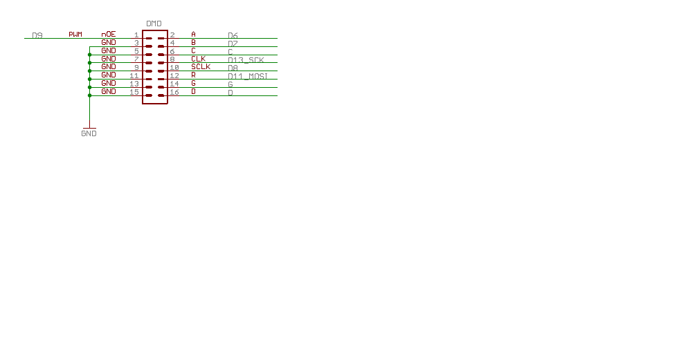
          Am trying to interface 32x16 DMD(single colour) to TM4c1294ncpdt controller. The 32x16 display driver is for aurdino boards but i want to use it for TM4c board.The communication is SPI.The Dot matrix display is connected to tiva board using DMDCon connector which has 16 pins. The display board has the Foll pins as shown in attachment

      1) A and B pins to select row(as only 128 leds can be on out of 512)

       2)R acts as MOSI

      3)there are 2 pins CLK and SCLK which am not sure to which I/O it should be connected.Clk is PIXEL clock and Sclk is like strobe pin.

      4)OE pin is for controlling all led high /low at a time (output Enable)

      5)pin C,G and D are NC and remaining are grounded.

      Have written the code to transfer some data on DMD but i am unable get any data.

please let me know

1)where i can find c library for 32x16 DMD 

2) Should i use Legacy Mode SPI or below code should work?

3)The Clk and Sclk difference 

 4)the configuration flow if anyone knows

have Used SSI3 


GPIOPinTypeGPIOOutput(GPIO_PORTQ_BASE, GPIO_PIN_4); //pq4 is oe pin 1
GPIOPinTypeGPIOOutput(GPIO_PORTN_BASE, GPIO_PIN_2); //PN2 is A pin 5
GPIOPinTypeGPIOOutput(GPIO_PORTJ_BASE, GPIO_PIN_1); //PJ1 is B pin 9
GPIOPinTypeGPIOOutput(GPIO_PORTE_BASE, GPIO_PIN_5); //PE5 is SCLK pin 13

Code *********Below is a test code which was for to display TI only using 8x8 .only.

#include <stdint.h>
#include <stdbool.h>
#include "inc/hw_memmap.h"
#include "inc/hw_ssi.h"
#include "inc/hw_types.h"
#include "driverlib/ssi.h"
#include "driverlib/gpio.h"
#include "driverlib/pin_map.h"
#include "driverlib/sysctl.h"

uint32_t ui32SysClkFreq;

#define NUM_SSI_DATA 8
const uint8_t pui8DataTx[NUM_SSI_DATA] =
{0x88, 0xF8, 0xF8, 0x88, 0x01, 0x1F, 0x1F, 0x01};

// Bit-wise reverses a number.
uint8_t
Reverse(uint8_t ui8Number)
{
uint8_t ui8Index;
uint8_t ui8ReversedNumber = 0;
for(ui8Index=0; ui8Index<8; ui8Index++)
{
ui8ReversedNumber = ui8ReversedNumber << 1;
ui8ReversedNumber |= ((1 << ui8Index) & ui8Number) >> ui8Index;
}
return ui8ReversedNumber;
}

int main(void)
{
uint32_t ui32Index;
uint32_t ui32Data;

ui32SysClkFreq = SysCtlClockFreqSet((SYSCTL_XTAL_25MHZ | SYSCTL_OSC_MAIN | SYSCTL_USE_PLL | SYSCTL_CFG_VCO_480), 120000000);

SysCtlPeripheralEnable(SYSCTL_PERIPH_SSI3);
SysCtlPeripheralEnable(SYSCTL_PERIPH_GPIOF);


GPIOPinConfigure(GPIO_PF3_SSI3CLK);
GPIOPinConfigure(GPIO_PF2_SSI3FSS);
GPIOPinConfigure(GPIO_PF1_SSI3XDAT0);
GPIOPinTypeSSI(GPIO_PORTF_BASE,GPIO_PIN_3|GPIO_PIN_2|GPIO_PIN_1);


//conf oE,A,B,Clk)/
SysCtlPeripheralEnable(SYSCTL_PERIPH_GPIOQ);
SysCtlPeripheralEnable(SYSCTL_PERIPH_GPION);
SysCtlPeripheralEnable(SYSCTL_PERIPH_GPIOJ);
SysCtlPeripheralEnable(SYSCTL_PERIPH_GPIOE);

GPIOPinTypeGPIOOutput(GPIO_PORTQ_BASE, GPIO_PIN_4); //pq4 is oe pin 1
GPIOPinTypeGPIOOutput(GPIO_PORTN_BASE, GPIO_PIN_2); //PN2 is A pin 5
GPIOPinTypeGPIOOutput(GPIO_PORTJ_BASE, GPIO_PIN_1); //PJ1 is B pin 9
GPIOPinTypeGPIOOutput(GPIO_PORTE_BASE, GPIO_PIN_5); //PE5 is SCLK pin 13


GPIOPinWrite(GPIO_PORTQ_BASE,GPIO_PIN_4,0x10);

SSIConfigSetExpClk(SSI3_BASE, ui32SysClkFreq, SSI_FRF_MOTO_MODE_0, SSI_MODE_MASTER, 10000, 8);
SSIEnable(SSI3_BASE);

while(1)
{

GPIOPinWrite(GPIO_PORTN_BASE,GPIO_PIN_2,0x0);
GPIOPinWrite(GPIO_PORTJ_BASE,GPIO_PIN_1,0x0);


GPIOPinWrite(GPIO_PORTN_BASE,GPIO_PIN_2,0x00);
GPIOPinWrite(GPIO_PORTJ_BASE,GPIO_PIN_1,0x02);


GPIOPinWrite(GPIO_PORTN_BASE,GPIO_PIN_2,0x04);
GPIOPinWrite(GPIO_PORTJ_BASE,GPIO_PIN_1,0x00);


GPIOPinWrite(GPIO_PORTN_BASE,GPIO_PIN_2,0x04);
GPIOPinWrite(GPIO_PORTJ_BASE,GPIO_PIN_1,0x02);


GPIOPinWrite(GPIO_PORTE_BASE,GPIO_PIN_5,0x20);
for(ui32Index = 0; ui32Index < NUM_SSI_DATA; ui32Index++)
{
//ui32Data = (Reverse(pui8DataTx[ui32Index]) << 8) + (1 << ui32Index);
ui32Data=0x01;
SSIDataPut(SSI3_BASE, ui32Data);
while(SSIBusy(SSI3_BASE))
{
}
}
}
}


  • Hello Kiran

    Can you please share the data sheet of the display module?

    Regards
    Amit
  • Hi,

                 The details about the display can be found in the link  below (Display name p10_1r_v701c)

                  http://cnlights.en.alibaba.com/product/60260384817-801533971/2015_new_inventions_p10_1r_v701c.html DMD-master.zip

    DMD_Getting_Started.pdf

  • Hi,
    Am also refering to the code package as below .The code is in cpp and Aurdino IDE but am trying to port it to c library in CCS6
  • Hello Kiran

    I do not see a specification on the interfacing protocol?

    Regards
    Amit
  • Hi Amit,
    Yes even am unable to get most of it,but after going through the DMD software driver ,i understood its SPI based.The actual driver is using Aurdino based board and the program is wiring based in CPP. i have attached the driver in the above post DMD-Master.zip file
  • Hello Kiran,

    Yes, that is true. Since you understand that it is a SPI Based protocol, the first thing would be to reverse engineer to understand when SPI transfer is being used and when a GPIO is being used for some special function. This will help create a "pseudo" spec for us to work with,

    Also an important thing is that the current budget for the 32x16 dot matrix seems high. Do make sure you have a good current source.

    Regards
    Amit
  • When Amit speaks to "current budget" he means the current demanded by that 32x16 Led Module.   That is typically many times that required by any Eval Board - and will surely "load down" your Eval Board's regulated supply.   An external supply is HIGHLY Recommended!  (especially during the debug process.)

    You must INSURE that a common ground is connected (and maintained) between the Eval board and your DMD.  (display)

    To "crack" the code of such displays - tie the data line high (or to the level intended to cause a pixel to glow) and then clock the display based upon the number of scanned pixels.   (as we don't know if yours is scanned horizontally or vertically - suggest that you start @ 32 Clocks.)   Does anything appear?   If not toggle the remaining clock pin.  (this may latch the data into the display buffer - required for display)   It may take several repetitions of such - each time w/you carefully noting the bit handling - and changing the polarity of the "latch signal/clock" - at some point pixel data should become evident.   The beauty of the "constant data level" is that we've reduced the data clocking to a, "Don't Care" condition.   (as the data never changes - clock upon EITHER edge is tolerated!)

    Being in the display biz - a 32x16 module is NOT too data intensive.   At best it can display 2 rows of 5x7 characters - or 2 "square" 16x16 ones.   Lcd modules are far less expensive - and eliminate the power requirement and extra effort to "tease out" display timing...

  • Hello cb1,

    Thanks for correcting the terminology of "current budget". The following statement in the PDF caught my attention.

    6. If or when you want the DMD to be very bright and the LEDs fully powered, connect a strong, stable 5V supply that is capable of at 4 to 40 Amps of current at 5V DC (regulated) to the large VCC (5V) and GND terminal block. The current used is proportional to how many LEDs are lit in the display.
    If all 512 LEDs are lit, the DMD is capable of drawing some rather high currents from the 5V rail! We recommend that for high brightness, high power use where most or all LEDs are lit, that an ATX PC power supply or similar is used to power the 5V rail. For more detail about high brightness 5V supplies please see our web page for the DMD.
    Do not use 5V from your Arduino or USB power to power the high brightness DMD 5V input terminals directly as those sources are only capable of 0.5A at best.
    If connecting separate 5V power to your DMD terminals while connected to your Arduino board by USB, be very careful of your external 5V power source polarity as you may feed damaging reverse voltage to your computer's USB port, should the wires be reversed or ground offset.

    Regards
    Amit
  • Amit - that (4+ Amps required) almost certainly explains poster's plight. I had to (read again) the initial post - to see if poster reported, "Working" (so rare that) while under Arduino. (he did not)

    So almost certainly power is an issue - and may be corrected w/proper power supply - creation of a common ground (between Eval Board & DMD) - and following the "locked data line" which I detailed earlier.

    Will be useful should poster (try) the test/verify procedure my earlier writing described - that has (always) worked - across many (abandoned/orphaned) displays. (provided they were adequately powered and commonly grounded)
  • HI,
    As per specification of DMD, only 128 leds can be lit out of 512,so using pins A and B am scanning 4 times to ON allthe leds.
    Example A B
    0 0 row 1,5,9,13 are on
    0 1 row 2,6,10,14 are on
    1 0 row 3,7,11,15 are on
    1 1 row 4,8,12,16 are on

    on setting A and B as above described ,am able to lit the rows
    i have used a separate 5v for DMD display and separate supply for tm4c1294ncpdt board.

    To make all leds high i am writing all 4 conditions in while loop

    while(1)
    {
    //scanning
    GPIOPinWrite(GPIO_PORTN_BASE,GPIO_PIN_2,0x0); port n pin 2 is A
    GPIOPinWrite(GPIO_PORTJ_BASE,GPIO_PIN_1,0x0); port j pin 1 is B


    GPIOPinWrite(GPIO_PORTN_BASE,GPIO_PIN_2,0x00);
    GPIOPinWrite(GPIO_PORTJ_BASE,GPIO_PIN_1,0x02);


    GPIOPinWrite(GPIO_PORTN_BASE,GPIO_PIN_2,0x04);
    GPIOPinWrite(GPIO_PORTJ_BASE,GPIO_PIN_1,0x00);


    GPIOPinWrite(GPIO_PORTN_BASE,GPIO_PIN_2,0x04);
    GPIOPinWrite(GPIO_PORTJ_BASE,GPIO_PIN_1,0x02);

    //scanning done

    GPIOPinWrite(GPIO_PORTE_BASE,GPIO_PIN_5,0x20);
    for(ui32Index = 0; ui32Index < NUM_SSI_DATA; ui32Index++)
    {
    //ui32Data = (Reverse(pui8DataTx[ui32Index]) << 8) + (1 << ui32Index);
    //ui32Data=0x01;
    SSIDataPut(SSI3_BASE, ui32Data);
    while(SSIBusy(SSI3_BASE))
    {
    }
    }
    }
    }

    So next i want to display Character on the DMD of any format,So i have configured SSI3 with below code

    GPIOPinConfigure(GPIO_PF3_SSI3CLK);
    GPIOPinConfigure(GPIO_PF2_SSI3FSS);
    GPIOPinConfigure(GPIO_PF1_SSI3XDAT0);
    GPIOPinTypeSSI(GPIO_PORTF_BASE,GPIO_PIN_3|GPIO_PIN_2|GPIO_PIN_1);


    //conf oE,A,B,Clk)/
    SysCtlPeripheralEnable(SYSCTL_PERIPH_GPIOQ);
    SysCtlPeripheralEnable(SYSCTL_PERIPH_GPION);
    SysCtlPeripheralEnable(SYSCTL_PERIPH_GPIOJ);
    SysCtlPeripheralEnable(SYSCTL_PERIPH_GPIOE);
    SysCtlPeripheralEnable(SYSCTL_PERIPH_GPIOH);

    GPIOPinTypeGPIOOutput(GPIO_PORTQ_BASE, GPIO_PIN_4); //pq4 is oe pin 1
    GPIOPinTypeGPIOOutput(GPIO_PORTN_BASE, GPIO_PIN_2); //PN2 is A pin 5
    GPIOPinTypeGPIOOutput(GPIO_PORTJ_BASE, GPIO_PIN_1); //PJ1 is B pin 9
    GPIOPinTypeGPIOOutput(GPIO_PORTE_BASE, GPIO_PIN_5); //PE5 is CLK pin 13
    GPIOPinTypeGPIOOutput(GPIO_PORTH_BASE, GPIO_PIN_1); //pH1 is SCLK


    GPIOPinWrite(GPIO_PORTQ_BASE,GPIO_PIN_4,0x10); have enabled OE high

    SSIConfigSetExpClk(SSI3_BASE, ui32SysClkFreq, SSI_FRF_MOTO_MODE_0, SSI_MODE_MASTER, 10000, 8);
    SSIEnable(SSI3_BASE);

    Next am sending Data through SSI3XDAT0 (MOSI ) pin.But am unable to see pixcels wrt to data passed ,all leds are on.
  • Hello Kiran

    You have to understand that

    1. I do not have the hardware that I can experiment with to understand the transaction
    2. I do not have still a specification that shows what the protocol is

    So, if you can use the existing software or speak with the manufacturer to get the specification, then it would be a very useful resource to get you going.

    Regards
    Amit
  • While (still) patently unclear - it (now) appears that some Leds are lighting. (I'd not "bet the farm on that.")

    Rather clearly - this is NOT a TM4C based posting - instead it is, "all about some foreign device - minus a real spec" - is this a proper usage of the TM4C forum?
  • HI Amit,
    Can i know which SPI mode is suitable for the my configuration?In my configuration , i am connecting the SSI3CLK pin from controller to CLk of my display and SSI3FSS pin in as chip Select ,so connected it to SCLK in Display .In my SPI ,am only sending data from MC to Dot matrix Display(MOSI)is required , no need of (MISO).So should i go for Legacy mode or TI SPI mode as the Operation of FSS is different in 2 mode.
  • kiran benni56 said:
    connecting the SSI3CLK pin from controller to CLk of my display and SSI3FSS pin in as chip Select ,so connected it to SCLK in Display

    That's doubtful!   Here's the typical (known good) hookup:

    MCU........................................Device

    SSIxCLK.................................CLK

    MOSI.......................................Data In

    SSIxFSS.................................CS

    Should (none) of the various SPI data formats "match" your display - you can use a GPIO - under (added) software control - to manage Chip Select (CS).

    I'm unclear as to your adoption of my past suggestion, "Tie the display data line high - then produce clocks - and observe the display for pixel arrival."   This has much value - I've designed/sold such displays (pre EBay) - it would be useful to follow such suggestions...

    *** Missing from this latest post is any mention of the (one assumes) data latching pulse - which is NOT part of any SPI scheme - and must be generated by an MCU GPIO.

    Details - details - yet this is your project...

  • Hello Kiran,

    You may use either of them: Legacy Mode or Advances Write mode.

    Regards
    Amit