This thread has been locked.

If you have a related question, please click the "Ask a related question" button in the top right corner. The newly created question will be automatically linked to this question.

DRV8353RH-EVM: Gate driver not working well

Part Number: DRV8353RH-EVM

Hello,

I have two DRV8353RH-EVM boards and am encountering same problem in both. I am using the default settings, I have not touched anything in the board.

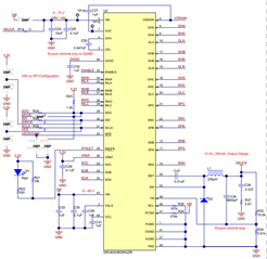
I am generating good INHX and INLX with Simulink for the 3x PWM mode (Default mode). I have measured values in oscilloscope and everything is fine in the ISOF28027 part. However, I am not getting GHX and GLX proper values. Many things are happening.

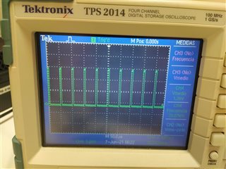
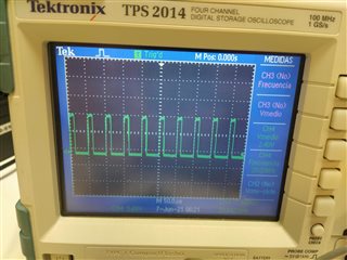
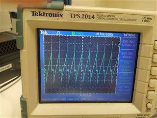
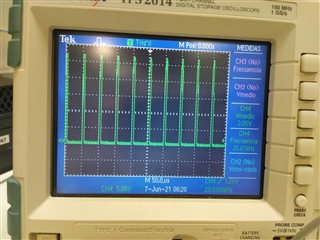
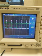
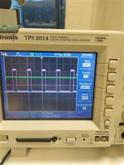
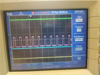
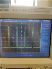
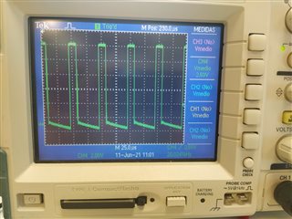
When i generate an ePWM of %50 duty cycle, for the three phases, I am getting a good result in GHA and GLA. B has no response at all and GLC is oscillating as it is supposed to be. GHC is getting some kind of triangular signal.

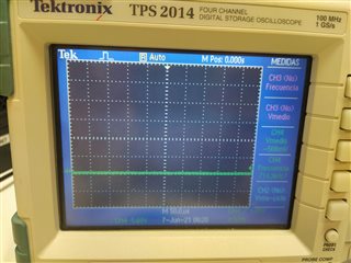
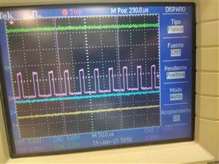
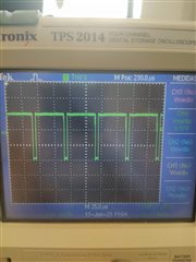
When different duty cycles are generated for each phase, we measure in GLC what it was supposed to be measured in GLB. GHC stays the same as before and GLB and GHC have no response. Once again, GHA and GLA work well.

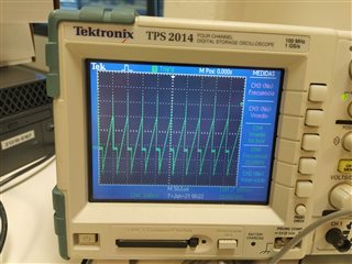
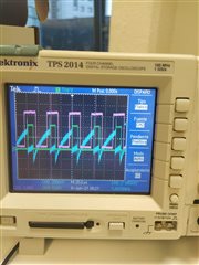
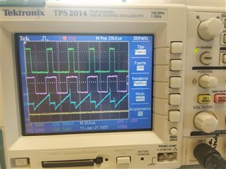
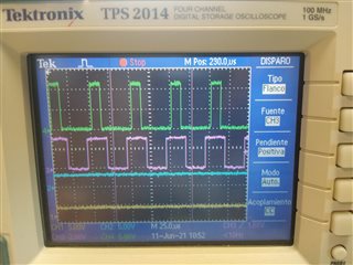
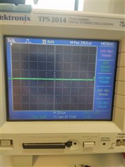
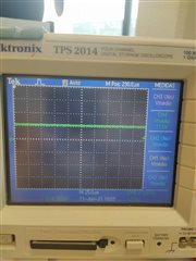
When sinusoidal reference is used, Phases A and B do have some kind of pattern, but it is not exactly the SPWM that it was supposed to be. Phase C stays the same, semi triangular GHC and GLC is constant at about 11 V.

I have been trying to solve the issue the past weeks but find no answer, it's been quite frustrating. I have found nothing in the forums. 

I really hope you can help me.

Jon

  • Hi Jon,

    Sorry to hear that you are having difficulty. Can you confirm the resistors on VDS, MODE, IDRIVE, and GAIN are the default that were shipped with the board?

    Do you have an oscilloscope waveform of GHA, SHA, and GLA that we can look at? As well as GHB, SHB, and GLB?

    Lastly, can you check the voltage present on the VCP and VGLS pins to ensure those regulators are up and running?

    Thanks,

    Matt

  • Hi Matt,

    Sorry for the late answer. I understand that this is the schematic we are using because we have touched nothing in the board. Therefore, the resistantces must be those in the schemaatic. If you need me to measure something you just need to ask.

    MEasuring voltages this is what I get for VM=15.6 V: VCP=26.4V, VDRAIN=15.6V and VGLS=12.1V.

    I have attached the oscilloscope images you asked for (images one by one and zip with every image), for every phase. I have one doubt, is the SHX the same as MOTX? I have measured the MOTX because looking at the schematic i didn't found out how to measure SHX otherwise. A has a duty cycle of 10%, B should have a duty cycle of 25% and C should have a duty cycle of %50.

    Oscilloscope Images.zip

    I really thank you the hel you are providing. I am so sorry to take your time.

    Looking forward to hearing from you,

    Jon

  • Hi Jon,

    Thanks for the data.

    You are correct that MOTx is the same as SHx. 

    When using 3x-PWM mode with sinusoidal control for this BLDC, the INLx pins are used to control whether or not the corresponding output phases are in Hi-Z (both high side and low side FETs off)  Speaking in logical terms: if an INLx pin is low, that means the FETs of the corresponding phase are in Hi-Z. If an INLx pin is logic high, then the output of the half bridge is controlled with a signal at the INHx pin. In this case, if INHx is low, the low-side FET of the corresponding phase is on, and if INHx is high, the high-side FET of the corresponding phase is on.

    In sinusoidal control, there will always be current flowing through either the high side or low side FETs of each half bridge. This means that there will be no Hi-Z states for sinusoidal operation (note: there will be a brief period of time where both FETs are off when the INHx is toggled from low to high or high to low, but this is simply due to the driver inserting dead time to ensure that both high side and low-side FETs don’t turn on at the same time). There will always be current flowing through each of the phases of the motor.

    Because sinusoidal control does not use Hi-Z states, we can tie the three INLx pins logic high. 

    Could you please provide me with the following (all on the same plot):

    - INLA, INHA, GHA, and GLA with respect to ground 

    - INLB, INHB, GHB, and GLB with respect to ground

    - INLC, INHC, GHC, and GLC with respect to ground

    I'd like to confirm with these plots that the input signals are what would we would expect for 3x PWM, as well as to confirm that the outputs are properly following the inputs.

    Best,

    Johnny

  • Hi Johnny,

    Thank you for helping me. I have attached the information you are asking for. Blue line is GHX, green line is GLX and pink line is INHX. As mentioned in the data sheet, as I am working with the 3x PWM, every INLX has been set; therefore they all have 3.4V constant value.

    Note that in the graphs every curve is scaled differently. I have done so, so that curves are comparable with each other.

    I hope the information provided helps. Anything you else you may ask, I will be pleased to send you.

    Thanks in advanced,

    Jon

    PS: It is surprising that I am getting in GLC what I am supposed to get in B (not sure if GHB or GLB, but GHL has same duty as expected in B).

    The following is phase A:

    Phase B:

    And phase C:

  • Jon,

    Could you probe the nFAULT pin during the phase B test and send me the result? I expect that there may be a fault that only shuts down phase B, or there may be some type of intermittent fault.

    Best,

    Johnny

  • Hi Johnny,

    I will attach the nFault signal picture in the oscilloscope, but it is a constant 3.4 value approximately. Only for clarification, i have created three different PWM for every phase but they are all working together. This is, every signal I sent you yesterday is working with a unique program and could be measured at the same time. I am sending this info because you mentioned the "Phase B test" and so as to let you know that every phase is working while I did the measurement.

    Another thing I wanted to tell you is that I have to boards, and in both is happening the same. I don't know if this helps.

    Thank you in advance,

    Jon

    The nFault signal:

  • Jon,

    We are not really sure why this behavior is occurring, the 3x has been tried on the EVM of this board many times with normal behavior. We understand that you've tied INLx high but, to confirm, could you please send us the following readings:

    The 'Phase B' test from earlier, but with the nFAULT pin also present on the reading

    The 'Phase C' test from earlier, but with the nFAULT pin also present on the reading

    INLB, INHB, GLB, and GHB with respect to ground

    INLC, INHC, GLC, and GHC with respect to ground

    We want to confirm that there is nothing wrong with INLX, as it is responsible for controlling the Hi-Z state of the half-bridges in this device. If there were problems in this portion of the device, the behavior you are seeing could occur.

    Just a note: the noise that you see on the GHC plot could be a result of noise caused by using a single-ended probe on GHC rather than a differential probe between GHC and SHC. Do you have a differential probe to measure between GHx and SHx?

    thanks,

    Johnny

  • Hi Johnny, sorry for the time it has taken me to answer you. I have attached everything you asked for. I don't have an oscilloscope with five terminals, so every signal with nfault is divided in two pics (see description below each photo).

    I hope this helps,

    Take care, 

    Jon

    Phase B tests

    INHB is pink. INLB is blue. GHB is yellow and GLB is green

    GLB is green. GHB is yellow. INHB is pink INLB is blue.

    GLB is green. nFault is yellow. INHB is pink INLB is blue.

    Phase C tests

    GLC is green. GHC is blue. INHC is pink INLC is yellow.

    GLC is green. nFault is blue. INHC is pink INLC is yellow.

    Measurements with differential probe:

    GHA with respect to SHA (MOTA)

    GLA with respect to SHA (MOTA)

    GHB with respect to SHB (MOTB)

    GLB with respect to SHB (MOTB)

    GHC with respect to SHC (MOTC)

    GLC with respect to SHC (MOTC)

  • Jon,

    Could you send a picture of your setup (board, test equipment, and motor)? Also, can you do the following test:

    Starting off with a the EVM, with nothing else attached: Supply voltage to Vm (such as 24V) to power up the board, apply 3.3V to just one of the INLx pins, apply a function generator supply to the corresponding INHx pin, and toggle that pin with the function generator with a square wave with between 0V and 3.3V. While doing this, measure the corresponding INLx, INHx, GLx, and GHx signals. Repeat this process for each phase. 

    Best,

    Johnny

  • Hello Johnny,

    Just to let you know, I am not using any motor in every measurement I sent. Every phase was open circuited, as I am intending to use this board as an inverter and not as a motor controller.

    With respect to the new measurements you are asking me, as I had nothing else but the supply voltage connected, I believe that the measurements you are asking for were sent last week.

    Sorry that it took me long to answer you,

    Thank you in advance,

    Jon 

  • Jon,


    The gate voltages show some overpumping (~14V) and negative voltages with respect to the source on LS FET of phase C. This is typically due to having too small of a gate drive current (IDRIVE) or not enough pulldown current when turning the MOSFET off to bleed off the gate capacitance of the MOSFET, which results in extra voltage pumping on VGLS.
    Could you try:


    - Removing R31 to place IDRIVE pin in HI-Z ( increases the gate drive current to 300mA/600mA)


    - Adding a stronger pulldown resistance between the gate and source by adding a 10k resistor at C8-C10 and/or C14-C16.


    See if these changes provide improved gate drive output waveforms.

    Best,
    Johnny

  • I edited this response with a bit more of an explanation. Just to letting you know.

  • Good day Johnny,

    Sorry for the late response. I will not be able to touch de board this week, but once I try to do tha changes you just explained, I will let you know.

    Thank you in advance,

    Jon

  • Hi Johnny,

    I just saw a pair of things. You are telling me to remove the R31, but, R31 is attached to VDS and not IDRIVE, isn't it? I have attached the photo.

    And the other thing is. We are intending to use this board's SPI after some modifications (beacause we got the DRV8353RH and not its RS twin). We were told to connect the R24,R28 and R30 so as to get an RS version instead of the RH. Moreover, they told us to select a GPIO to play the role of the nSCS (we don't know how to do this yet neither, but it still doesn't urge) . Will this have any impact on the suggestions you made?

    Thank you in advance

  • Hi Jon,


    What you said about R31 is true. This is my error. You should remove R26 to put the IDRIVE pin into HI-Z for the hardware variant.


    Regarding what you said about using this board for SPI: It is important to note that you need a DRV8353RS chip along with the SPI board configuration in order to use SPI functionality. When you switch over to a SPI device, you will be able to change your IDRIVE and other parameters via bit registers instead of external resistors. In order to change the EVM from a hardware setup to a SPI setup, you will need to have a DRV8353RS chip soldered in place of the DRV8353RH chip, and you will need to populate and remove the appropriate resistors in order to configure the signals correctly. You can reference the SPI-variant EVM schematic attached to this post to see which resistors should be populated and DNP for the SPI configuration.


    Also, regarding my request from 10 days ago: the reason these tests would be helpful is because we want to eliminate the possibility of the issue being with the Simulink setup. In order to confirm this, you could perform the tests described in that post with a function generator on only one phase at a time (applying it to only one of the INHx pins, while holding the corresponding INLx pin high), while measuring this phase's output. Also, a picture of your setup could still prove useful. When you get the chance, can you perform these tests and attach a picture of your setup?


    Best,
    Johnny

    MD016A(001)_Sch.PDF

  • Hi Johnny,

    While doing some of your proposed tests I think I found the problem. On the one hand, it is neccesary to set the MODE pin to 0 so as to get a good PWM. For some reason it was not always 0, and the PWM failed.

    However, after explicitly setting this pin voltage to 0, I found that for great frequencies of commutation, the gate driver needs  time to set the GHX pins high. Therefore, it seems that once qe remove the R26, everything will work correctly. Even though I won't be able to remove the resistor until next tuesday, I will let you know, then, if we have achieved anything.

    Regarding to the SPI connectiom, we intend to recieve some info in the F28027F via SPI from another peripheral. The fact is that we bought the boards before SPI was planned to be used with these, and we want to accomodate this boards to use SPI connection with another peripheral. Of course, SDO must be untouched and set to 0 as it is the same node as MODE. However, we just need the recieving pin, SDI. I was thinking that maybe it is possible to make the connection directly from our peripheral to the ISO F28027F pins. Do you believe this will be possible?

    I attach the picture of  my setup below.

    Jon

  • Jon,

    Due to the internal circuitry, as shown below, the voltage of the MODE pin will not be 0V during 3X PWM. The presence of the external 47K resistor in combination with the internal resistor divider will set the MODE pin to a specific voltage, which tells the driver what mode to put it in. You should see about 1V or so on the MODE pin in 3X PWM mode. By tying the mode pin to 0V, you are effectively placing the device in 6X PWM mode.  As seen on Figure 38 of the Data Sheet for this device:

    To achieve 3X PWM, you would place a 47K resistor between the MODE pin and ground (the EVM comes like this).

    There is a good chance that if you have the launchpad connected, the GPIO connection between the MCU and the MODE pin could interfere with the voltage at this pin, causing undesired/unexpected PWM mode(s). You mentioned that the voltage at the MODE pin is not always 0 Volts. From what you are saying, it seems like the voltage is toggling between some voltage and 0V on this MODE pin in some way. This could be due to the MCU GPIO attempting to control the MODE pin in some way, which could result in the driver switching between modes in the middle of operation.

    When the voltage was not 0V, what voltage(s) were you seeing, and how often was it at 0V and the other voltage(s)? As mentioned before, you should see a constant voltage of 1V at the MODE pin if the device is in 3X PWM mode. Since the launchpad could be attempting to change the voltage at the MODE pin, it would be best to remove the launchpad connection when performing the tests mentioned in my last post (with a function generator on one phase at a time), to eliminate this possibility.

    This may not be an issue with the IDRIVE setting, so removing R26 might not be necessary here.

    Best,

    Johnny

  • Hi Johnny,

    Hope you are doing well and sorry for my late response.

    We have partly resolved the problem with the PWM. We have just found out that setting MODE to 0 and using PWMx6 is working well, so we have decided we will use it for now. Do you see any inconvinient?

    However, regarding to the SPI connection, we intend to use it, as I believe I already said, with a peripheral directly connecting it to the F28027. The fact is that MODE pin and SDI are connected, so both have same tension. Is there any way to break this connection and use them separately? I attach a picture with the schematic of the ISO F28027F.

    Thanks to this, we would not have SDI and SDO connected to the Driver Stage and we could use the SPI connection of the Microcontroller, independently. We would need to choose other GPIOs to play the role of nSCS but this is possible by choosing some other GPIO which are not used.

    Do you think that this will be possible?

    Thanks in advance,

    Jon

  • Hello Jon,

    I'll have an answer for you by the end of tomorrow.

    Best,

    Johnny

  • Hi Jon,


    Using 6x PWM is fine as long as your code supports it correctly.


    Yes, the configuration you mentioned is possible because you are using a hardware device. The SDI, SDO, and SCLK pins on your MCU will not be connected to DRV, because in your case, these DRV pins are configured via external resistors as seen here (DRV8353RH EVM - your device) and the 0 ohm resistors are depopulated that connect the SDI SDO, and SCLK, pins of the F28027 to the DRV:


    Since you are doing 6x PWM, you can tie MODE to ground. You don't need it to be connected to the MCU. This can be done by depopulating R22 and swapping R23 out with a 0 ohm resistor to ground.


    The problematic pin for your configuration is the nSCS/GAIN pin, because it is directly connected to a GPIO of the LAUNCHXL without a 0 ohm resistor to disconnect it from the MCU. For the hardware device, the GAIN pin is used to set the CSA gain. This doesn't need to be connected to a GPIO as it can be set through a resistor to ground or a resistor to DVDD (depending on the desired setting), but unfortunately this trace does not have a 0 ohm resistor that could be removed to disconnect the trace from the GPIO. As you mentioned, the solution for this issue would be to program a different GPIO on the MCU for the function of the nSCS pin.


    Best,
    Johnny

  • Good day Johnny,

    I write you to let you know that you resolved every doubt and issue we had with the board. Therefore, I think that this conversation can be finished.

    I really appreciate the help you have provided and the patience you had. Thank you very very much.

    Stay safe and take care,

    Best regards,

    Jon