This thread has been locked.

If you have a related question, please click the "Ask a related question" button in the top right corner. The newly created question will be automatically linked to this question.

DRV8432: VREG disturbances cause Overcurrent and undervoltage protection to trigger

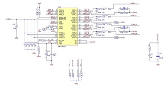
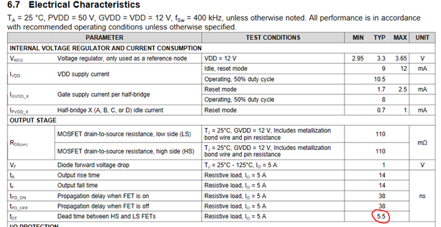
Part Number: DRV8432

Hello,

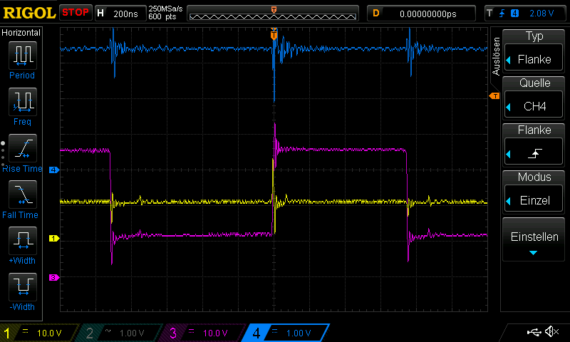
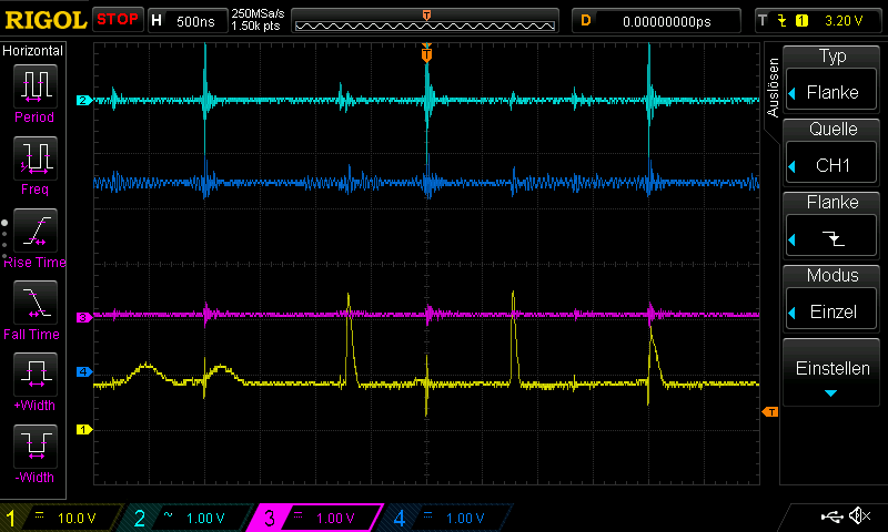
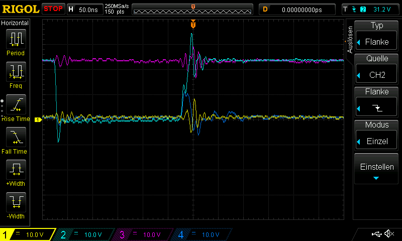
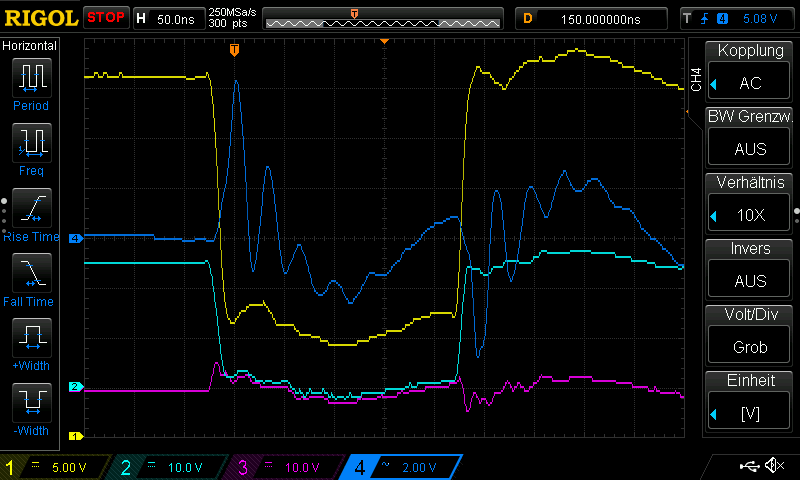
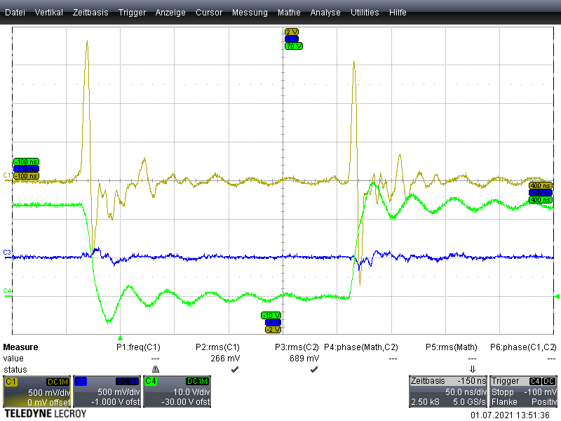
due to the switching edges of the FET's there is a ground rise between AGND and GND.
Measured with the oscilloscope there are voltages of 2V peak-to-peak between GND and AGND.
In my opinion, this circumstance leads to the fact that the input signals are not correctly detected.
We have already placed a 1nF and a 150nF capacitor between VDD and AGND.
Do you have any recommendations how to minimize this influence?

Best Regards

  • Hi Kai,

    Thank you for posting to the forum.

    The OC_ADJ requires a resistor connected to AGND to set the overcurrent limit. If AGND is offset by 2V, the overcurrent fault will be triggered at a lower limit.

    I would have to look at your schematic to understand what can be causing the voltage difference between AGND and GND. Are you able to share the driver schematic?

    Is AGND and GND connected directly on your design? If a resistor is placed, that could explain the voltage difference between the two grounds.

  • Hello,

    thank you for the fast response.
    AGND and GND are connected via a 1 Ohm resistor as described in the datasheet.
    The circuit diagram is derived from the TI Eval board.
    Is it correct that the PWM_A to PWM-D, RESAB, RESCD, FAULT and OTW signals refer to AGND?

    Here is the extract from the schematic.

  • Is it correct that the PWM_A to PWM-D, RESAB, RESCD, FAULT and OTW signals refer to AGND?

    That's correct. These signals are powered by the VREG output which is referenced to AGND. However, we recommended connecting these signals to GND if AGND and GND are connected either directly or by a 1Ω resistor as shown in the EVM design and datasheet.

    Can you connect AGND and GND directly. That should help fix the grounding offset. If this does not work let me know and I can provide you with more assistance.

  • I have connected AGND and GND via a 0 Ohm resistor.
    The problem still exists.
    I have attached a screenshot, there you can see the voltages at BST_A(Yellow) , BST_B(Red), and VREG(Blue) related to GND.

    Do you have any other suggestions?

  • Hi Kai,

    I have connected AGND and GND via a 0 Ohm resistor

    Just to confirm, Is the issue of the of the 2 V-peak-to-peak between the AGND and GND present? Or is it just the issue of the driver not functioning correctly? Can you provide a waveform of the AGND to GND voltage? Try using the spring hook on the voltage probe for more accurate measurements.

    Unfortunately, the screenshot doesn't provide much more useful information. There are some large spikes in the VREF trace but they last for a very short time. However, if the VREF drops very LOW, it could cause malfunction in the driver. All of the digital circuitry of the driver runs on the VREF voltage. If the VREF voltages drop, it may cause the driver to not function properly.

  • I think the problem is that the internal comparators in the DRV8432 detect a wrong level due to the disturbance of the VREG. The reason for this disturbance is probably that the BST pins go to a voltage close to 0V.

    How can this be prevented?

    Attached is the desired screeshot with direct connection of AGND and GND.
    AGND to GND (Blue)
    BST_A(Yellow) BST_B(Red) to GND.

  • Hi Kai,

    Thank you for providing the scope images I requested. The AGND to GND voltage is very unstable and which will cause the VREF voltage to become unstable as well. As I mentioned previously, if the VREF signal is not stable, the internal circuitry may not function properly.

    I wonder if somehow the device has been damaged. Have you tried replacing the IC with a new one? If not, can you please try that and observe if the VREF becomes more stable. I suggest not connecting the motor first to verify that the driver is working properly. Then connect the motor and try to drive it.

  • Regarding your question: We have tried different drivers with same behavior.

    I have made further measurements.
    In the attached scrennshot you can see the following voltages:
    Yellow = BST
    Red = GND
    Dark blue = VREG
    Light blue = GVDD (AC coupled)

    As you can see, BST has a level of about 8V.
    In my opinion, BST behind the diode should have at least 11V.

    I currently have no explanation for this behavior...

  • Hi Kai,

    Thank you for providing the information. I'm also a bit confused as to what is causing the BST voltage to be lower. Although the waveform is very odd. There are times when it seems to peak at around 25V.

    There also seems to be a lot of AC coupling in GVDD. It may be that there is some noise coupling in your PCB.

    Please give me around 24 hours to investigate these results. I want to take some more time to fully understand what the root cause of the low BST voltage and GND offset.

    Thank you in advance for your patience.

  • Hi Kai,

    I'm still investigating. Please give me another 24 hours.

  • Hello,
    there is more info about the problem.
    At the moment of switching there is a voltage increase at the OUT-pin. See attached picture.

    Shown are the different OUT-voltages measured against GND.

  • Hi Kai,

    Can you let me know what each of the traces on the scopeshot are?

    It is expected for the output current to increase when switching. If the layout is not optimized and the high di/dt loops are not minimized, there can be some ringing oscillations which can cause the voltage to increase. A way to minimize these oscillations is to add snubbers or minimize the high di/dt loops.

  • As described, OUT_A, OUT_B, OUT_C and OUT_D voltages can be seen.

    They were measured referenced to GND.

  • Hello

    we currently assume that the Mos-FET's in the DRV8432 are switching simultaneously and that is why the PVDD and GND potential is oscillating.

    We have removed the load and the filter,
    then we connected a resistor of 1200 Ohm between the OUT_Pins and GND to charge the bootstrap capacitance of the HIGH-Side FET.

    Even in this configuration, the operating voltage has a momentary dip.

    Attached is a picture which shows this case and the related voltages:
    Dark blue = PVDD=24V (AC coupled)
    Light blue = OUT_A
    Red = OUT_B
    Yellow = BST_A

    All measurements are related to GND.

  • Hi Kai,

    Oscillations at frequencies around 20-50MHz that can be seen on PVDD and OUT_X  are probably caused by parasitic inductances of PCB traces and components and high di/dt. Pablo has already mentioned ways to deal with that problem.

    I would focus on PCB layout, DRV8432 is quite compact device what can make PCB design challenging for higher currents. Additionally you added current sense resistors which bring additional parasitic inductances and make design even more complex.

    Output rising/fall times for DRV8432 are around 14ns what is really fast and makes PCB layout critical.

    If you can share your PCB layout for a review or probably you should be able to send it privately to TI engineer.

    Regards,

    Grzegorz

  • Hi Kai,

    I agree with Grzegorz. This could be an issue with parasitic components on the board causing the oscillations on VM. If you can share you PCB layout via private message i will happy to review it and provide recommendations for improvement if needed.

  • There are no inductances in the output for the shown oscillogram. We removed the filter on the output and also removed the motor. From my point of view, all power-carrying parts were eliminated until only the DRV8432 remained. For testing purposes the 1200 Ohm resistor was connected in parallel with the low-side MosFET.
    The Dark blue = PVDD=24V (AC coupled) in the oscillogram from the previous message is the 24V_POWER_in voltage. By the 1200 Ohm resistor, output current is 20mA.

    Regarding Grzegorz message: The current sense resistors should not be able to have influence, when the motor is not connected.

    That's why we assume that the Low and High-Side Mos-FET's of one half  bridge in the DRV8432 are switching simultaneously. In this case the power supply will be shorted for a few ns.

    Could you please explain the meaning of tDT in the below picture?

  • Hi Kai,

    If you suspect cross-conduction I would try to measure voltage on sense resistor (spring hook connected directly to GND side of sense resistor). It may give some answers, though for these frequencies resistor will be an RL circuit and additionally even spring hook can pick up some noise.

    You are right, without output current sense resistors should not play a big role. There is no output current but Mosfets have output capacitance and some current flows during switching operations in half bridges. Its hardly to say if that current can cause such ringing.

    There are quite a lot of strange things that happen on your board, maybe using DRV8432EVM for initial tests would be a good option and then if everything works well DRV8432 could be replaced with ICs that you have problem with. That would show if problems are caused by you board or DRV8432s.

    Regards,

    Grzegorz

  • Hi Kai,

    Thank you for the information.

    Could you please explain the meaning of tDT in the below picture?

    This is the dead time inserted when the FETs are switching to prevent both FETs of a half-bridge from conduction at the same time.

    There are quite a lot of strange things that happen on your board, maybe using DRV8432EVM for initial tests would be a good optio

    I agree with Pelikan. You should try to test the load with the EVM under same configurations as your board. If no issue is observed, it propably means there might be something not right with your PCB.

    Another thing you can try is replacing one of the ICs on the board with a new one and see if the issue follows the IC or PCB.

  • Hello,

    thank you very much for both answers.
    The measurement setup is again without load, and 1200 ohms are connected in parallel to the low-side MosFET.
    As suggested, we measured across the current sense resistor(0.01 ohm) and find a very high current flow in the switching moment.

    Attached is another oscillogram with the following voltages:
    Yellow = voltage across current sense resistor
    Green = Switching edge at OUT_C
    Blue is a short-circuited probe at GND of the current sense resistor, as GND reference to detect the error in the oscilloscope channel.

    OUT_C reaches -8V after the falling edge.
    This voltage should not occur due to the internal diode on the low-side MosFET.

  • Hi Kai,

    Thanks for these waveforms. 

    Can you tell what is the size of sense resistors (0805, 1210 etc.)?

    Regards,

    Grzegorz 

  • Kai,

    Thanks for the information.

    Are you amplifying the voltage at the the SENSE resistor? or are you measuring the voltage right at "MEAS_AB" or "MEAS_CD"? if so, the current is around 175-A which is very large. I suspect this may cause damage to the driver. Have you tried replacing it with a new IC? Does that help?

  • Hello

    we have a 2nd board connected with the same behavior. The voltage was measured directly across the MEAS resistor.
    The type of MEAS_AB and MEAS_CD resistors can be seen in the following link.
    https://docs.rs-online.com/3094/0900766b8002e768.pdf


    Today the DRV8432 Eval board arrived. We will put it into operation and perform further measurements.

  • Hi All,

    First sinewave on sense resistor has period of around 18ns so its frequency is around 55MHz. Its hardly to find any information on ESL value of resistors but some manufacturer says its low inductance SMD current sense resistors have ESL of 0.5-5nH. Lets assume in this case ESL of sense resistor is around 2nH what gives its reactance

    xl = 2 x Pi x f x L = 6.28 x 55 x 10^6 x 2 x 10^-9 = 0.69 Ohm

    Reactance of sense resistor is much higher than its resistance 0.01 Ohm and it will cause the main part of voltage drop on that sense resistor during such fast peaks/ringing. I can only guess peak current causing these single sinewaves is somewhere 1-10A. Looking on timing of these single sinewaves and that current 1-10A is rather not caused by switching of output mosfet capacitances I also think cross-condution may happen for a couple of ns. Now,why this may happen:

    - DRV8432 timing is close to critical and it may be normal for them to have that very short cross-conduction period, during normal work di/dt caused by switching operation and reverse recovery of mosfets body diodes can cause even higher voltage peaks on sense resistors,

    - cross conduction may be caused by non-optimal pcb layout that interferes with IC timing and its "Intelligent Gate Drive and Cross Conduction Prevention"

    - it may be caused by DRV8432 damage.

    I think using DRV8432EVM board would allow to exclude some of above mentioned possible causes.

    All above are just my thoughts and I may be wrong.

    Coming back to "OUT_C reaches -8V after the falling edge.
    This voltage should not occur due to the internal diode on the low-side MosFET" - that voltage drop is caused mainly by di/dt and parasitic inductances of sense resistor, DRV8432 and pcb traces. That is why pcb layout is very important in case of fast switching mosfet circuits. DRV8432 has rising/fall times around 14ns what is pretty fast and every single 1mm of pcb trace matters as well its parasitic inductance.

    Regards,

    Grzegorz

  • Hi Kai,

    Its a bad choice for a sense resistor for high speed switching mosfet circuits. Their ESL is probably very high, much better choice are SMD resistors like 1210, 2512, even better are these with wide package like 1020, 1225 or special made low inductance current sense resistors. Ground plane close under current sense resistor as a reference plane may also help to limit parasitic inductance of sense resistor.

    The current 1-10A that I mentioned in my previous post probably is much lower because of high ESL of that sense resistor.

    Hopefully EVM board will bring some answers and positive results.

    Regards,

    Grzegorz

  • Kai,

    Agree with Grzegorz on the selection of the sense resistor.  We have seen issues before with high ESL sense resistors.  

    I am going to close this post for now pending results from your EVM analysis.  Please just repost any questions.  If thread is locked, please just click the "ask a related question" button.

    Regards,

    Ryan