This thread has been locked.

If you have a related question, please click the "Ask a related question" button in the top right corner. The newly created question will be automatically linked to this question.

DRV8662: Output Load and Boost Current Limit

Part Number: DRV8662
Other Parts Discussed in Thread: LM48560, DRV2700

Hi,

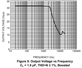
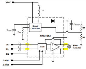
I am trying to use the DRV8662 to drive a 1uF PZT up to 12Vp2p. I have set the gain setting to 00, FBB to 36.7k and FBT to 300k.

RSET pin set to maximal BST current limit, I have noticed in above setting, the boost's avg input current is clamped at around 300mA, this happens at 3kHz, as I increase the driving signal's freq, the avg current limit will not increase anymore.

I have also noticed, when I configured FBB to 36.7k, FBT to 507k, the boost's avg input current is clamped around 500mA.

There is no such thing in the datasheet talks about the boost current delivery capability, could you please help?

Do you have better recommendation of a better device to drive my PZT? for up to 4kHz input freq.

Thanks,

Max

  • Hello Max, 

    The boost current is dependent on the output voltage, boost voltage, and load. There is also the boost current limit that can be programmed by Rext. What value of resistor are you using for this/what is the boost current limit set at for your application? Just to clarify on the current, when you say boost input current, where are you measuring the current? 

    For your application, is 12V peak to peak the maximum output needed? If so, you might have better performance with our LM48560 piezo driver based on your piezo load and frequency requirements. We have data for a 1.5uF load as can be seen here: 

    Best Regards, 

    Justin Beigel

  • Hi Justin,

    Thanks a lot for your explanation. Input current I am referring to input DC current or the current draw from power supply, this current is also the boost inductor's avg current. Since 8662 is DCM controlled, the peak current is clamped around 2.5A? you are correct, as I increase the BST Vout, the input current (avg current) does go up.

    The thing is I am testing couple PZT to see which one is better for me, the 1uF PZT I asked initially doesn't need high voltage, 24Vp2p is the spec limit from manufacture, I also have low capacitance PZT like 100nF. Fig 9 of the device you recommended, it seems it will auto attenuate the VBST output when input frequency is higher than 2.5kHz? Does this device has any similar mechanism to reduce VBST VS input frequency?

    BTW, why there are 2 pairs of input+/-? there is only 1 BTL amp to diff drive the PZT.

    Thanks a lot for the help.

    Max

  • Hi Justin,

    One more question, what is the sole purpose of ACL function? is it more related to the boost Vout envelope tracking or it's more input signal frequency dependent? is figure 9 also related to the ACL function? From fig 15, ACL function will limit the boost output voltage based on input signal voltage, if that's true what is fig 9 mean?

    Thanks, Max

  • Hello Max, 

    For the figure I shared, the load was 1.5uF so I would expect the VBST to be less attenuated for your 1uF load and be able to go to a higher frequency when using 24Vp2p. 

    The two different input pairs can have their gain stages configured differently and can be switched between if desired. This allows to switch between input sources or switch gain settings quickly. 

    I am looking into your other questions and will have feedback for you shortly. 

    Best Regards, 

    Justin Beigel

  • Hello Max, 

    Here are some answers to your remaining questions:

    The boost current can also be limited by the value of Rext. You are correct that this is limited to about 2.5A at a maximum. 

    The ALC function on the LM48560 limits the peak output voltage and the peak boost voltage. This is to eliminate any potential overshoot of the desired output voltage. In other words, you could clamp the output to limit at 24Vpp and any input that would cause it to go higher would be limited. 

    Best Regards, 

    Justin Beigel

  • Hi Justin,

    Thanks a lot for digging the answers for me, much appreciated.

    1 last question if you don't mind, the DRV8662 seems to be a Class A type PA when I tested on the bench, do you mind to confirm the class of PA?

    Best regards,

    Max

  • Hello Max, 

    The DRV8662 is a class AB amplifier. 

    Best Regards, 

    Justin Beigel

  • Thanks Justin, but not BTL class AB?

  • Hi Xinyu,

    I'm not clear about your question, DRV8662 has BTL (differential) inputs and outputs:

    Best regards,
    -Ivan Salazar
    Applications Engineer - Low Power Audio & Actuators

  • Hi Ivan,

    Thanks, i tested the device with a 1uF piezo and a pure differential sin wave input, the differential output does not swing to GND, the output rather swings between a intermediate voltage. Also due to the boost converter architecture, boost output is very dirty meaning a lot ripple, and this ripple couples into the diff PA.  

    DRV2700 just support Flyback config VS DRV8662? Should be very similar devices right?

    Thanks a lot.

    Xinyu

  • Hello Xinyu, 

    The boost does have a ripple based on how it operates but the ripple cancels out when looking at the differential output since it applies to both +/- sides the same. 

    You are correct that they are similar devices and the Flyback configuration support is a key difference between them. 

    Best Regards, 

    Justin Beigel

  • Thanks Justin,

    Just want to share this scope capture, input is 1.8Vp2p, Gain setting to 00,Vboost to ~18V, yellow is OUTA (5V/div), green is OUTB (5V/div), blue is VBOOST (5V/div), CH4 is IOUTA (50mA/div), the light pink is OUTA-OUTB (10V/div). DRV8662 EVM.

    Look at the boost trace, it's not AC coupled, so much noise, I agree to what you are saying, but seems it still couples into the PA. Also the yellow and green traces are not able to swing to GND.

    Best regards,

    Max

  • Hello, 

    I see what you mean about the noise. That does seem more than expected. I will do some testing to duplicate this in the lab but need you to confirm a couple things first. 

    1. This looks like a triangle waveform, is that correct or is it a distorted sine wave? 
    2. What is the frequency of the input signal for the capture you showed? 
    3. Was this using your 1uF load? 

    Best Regards, 

    Justin Beigel

  • Hi Justin,

    1. I injected perfect sin wave via function generator, the output is distorted, I think it's due to the lack of current capability of DRV's boost

    2. 1kHz I believe

    3. It's an actual PZT speaker with 1uF internal cap

    It's an old device , i dont think it's meant for >300Hz, just my thoughts, and I already reduced the boost voltage quite low to reduce unnecessary efficiency hit.

    Best regards,

    Max

  • Hello, 

    You are right that the performance is better at lower frequencies. I did some testing with a 1uF capacitor as the load and there was noticeable attenuation on the signal between 300Hz and 1kHz but I never had the sine wave distort. Are you using the EVM during your testing or a different board? If you are using an EVM, I think if you adjust the boost voltage higher, you might get a cleaner sine wave on the output. 

    Best Regards, 

    Justin Beigel