This thread has been locked.

If you have a related question, please click the "Ask a related question" button in the top right corner. The newly created question will be automatically linked to this question.

DRV8353F: Continued current sense problems

Part Number: DRV8353F
Other Parts Discussed in Thread: DRV8353,

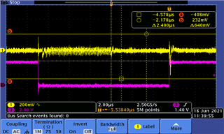
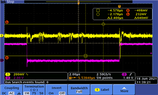
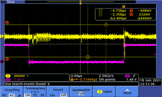
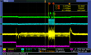
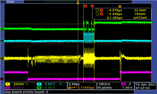
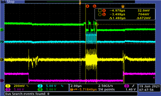
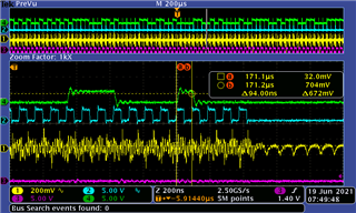
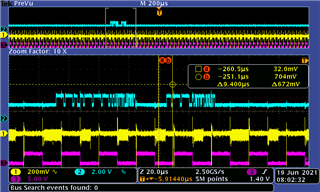
With all the layout changes suggested before, I have the exact same current sense problem as I had in the previous iteration.  Here are snapshots of the current sense line AC coupled along with the gate drive signal.

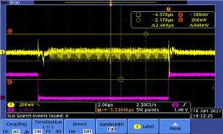
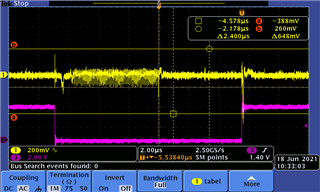
No real changes from the last time.  Occasionally one or more channels have noise for the entire duration, and sometimes only to the halfway point.  My layout looks like the following (which is basically the same as the one I posted at the end of the last thread):

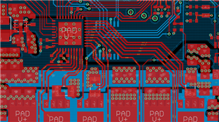
I'm not too surprised that the layout problems didn't fix anything, as the same basic layout did not exhibit this problem with the DRV8323RS based design I previously had.  No doubt this is better, but whatever the problem is, it did not resolve it.

Any other ideas?  

  • Also, as before, the behavior varies between boards, but is consistent for each board. 

     * The noise never seems to be present on channel C, just A and B.
     * It is present even when there is no motor connected (and thus the current is always 0 through the output)
     * There are a few other modes that the noise can be present in beyond the two scope captures from above.  Sometimes it is slightly lower in magnitude, and sometimes it is less consistent over time and sometimes it decays before reaching the halfway point.  However, in each case, each board/chip seems to have its pattern between channels A and B and sticks to it.  i.e. channel A on board 1 is either always large magnitude, low magnitude, or intermittent.
     * I'm not sure I've seen a "low-magnitude" channel ever have noise during the entire cycle, it always seems to stop at the halfway point if it is present in a particular cycle.


    A "low-magnitude" channel:

    An "intermittent" channel:

    And a channel that "decayed" before reaching the halfway point:

    I am happy to share my full design files if that is helpful to look for other problems.

  • Hi Josh,

    Previous related post: LINK

    Sorry to hear you are still having issues. 
    Please provide the full design files so we can look through them. If you want to provide them over email that is OK. 

    I will review this with others team members and get back to you tomorrow at the latest. 

    Thanks,

    Michael

  • Michael,

    What is the best email address to use?  (Not sure if it is more appropriate to find some DM mechanism here at E2E)

    -Josh

  • Hi Josh,

    Make sure to let me that you got into contact with Michael!

    Thanks,

    Matt

  • Hi Josh,

    If noise occurs with no motor output current then probably source of problems lays outside Mosfet bridges. Looking at 4-th and 5-th waveforms from previous post I can see some patterns in the noise, it looks a bit like serial communication. Noise on 6-th waveform (200ns time base) looks like 7-8 bits + 2 bits signal.

    Maybe it would be worth to check all pins related to communication on DRV8353 and MCU as well power supply pins if there is any noise/signal similar to noise on SOA and SOB outputs and occurs at the same time.

    Probably it is a wrong direction but SOC trace that does not experience problems with noise lays further from SPI bus than SOA and SOB traces. On 11.2 layout example SOX traces are shielded by GND traces.

    It would be good to know at what frequencies work all clocks in MCU (CPU, Peripheral, SPI etc.) as well digital core in DRV8353F. Maybe one of them is close to 13MHz.

    Regards,

    Grzegorz

  • In this application, the DRV8353F SPI is not used during normal control, only if a fault is triggered and during setup.  So those lines are driven to fixed values during all this.

    There is another set of SPI lines that runs on the opposite side of the board to a magnetic encoder at 10MHz. (Maybe closer to 10.6MHz in practice).  I don't *think* they are the cause, because they are separated by a ground and power plane from any relevant signals, and if anything are more lined up with the SNC input signal.  Scope traces show that they seem to be unrelated.  Here are three traces from different cycles in the same setup (so the different noise profiles are just what happens in steady state operation for this SOB channel).  The encoder SPI is teal and green, while magenta is the motor drive and yellow is the SOB output.  The noise on SOB during the SPI cycle is just coupling between scope probes, it disappears if I disconnect the SPI probes.

    And finally, a close up to see the cycle time:

    The only other digital signals that change state on this board during normal operation is a CAN-FD bus which runs at 1Mhz/5Mhz.  It doesn't seem correlated with anything either.  Here is a plot of it going (across multiple cycles) in teal.  You can see some cycles with noise across the entire low drive cycle and some with it across half, none of which seems to line up with the CAN-FD bus.

    What clock rates does the DRV8353F use internally?

  • If noise does not come from pcb traces then it may come from inside of DRV8353 or MCU. I would try RC filters like 1 kOhm + 100pF placed on SOA and SOB traces between DRV and MCU, they should keep noise withing source. Then if noise is still present it may be possible to tell if it comes from DRV or MCU.

    Grzegorz

  • Hi Josh,

    I see that there is no RC filter on the outputs of SOx. We recommend that you add these to filter out high frequency switching noise. 

    Please place the RC filter as close to the MCU as possible so that no noise is coupled into ADC inputs of the MCU. The RC filters should be placed BEFORE the test points and ensure the test points are as close as possible to the ADC inputs of the MCU.

    Test points can cause extra inductance and noise that can couple over from any layer of the board into the SOx signals. Such as the SPI signals that were mentioned from the pervious post on the bottom layer of the board.

    One suggestion I'll make is removing the test points and blue wire directly to the ADC inputs. 

    I hope this helps.

    Thanks,

    Michael

  • Well, I know the test points aren't a problem, because the first iteration of this board had no test points on those lines but failed in the same way.  The traces for SOX are only 1cm long, directly routed from a low impedance amplifier on the DRV8353F to a high impedance ADC input on the MCU.  There are no SPI transitions happening anywhere near in time to when the noise is happening, and there are no SPI lines particularly close to the test points either.

    I'll blue wire in an RC filter to verify my suspicion that the noise is not coming from the MCU, but from the DRV8353F.

  • Well, I might be getting closer.  Using a 120ohm + 1000pF RC network did clear up the problem, but not because it was filtering.  It seems to have stopped the output of the DRV8353F from becoming unstable as well. In fact, just placing a 1000pF capacitor on SOX seems to resolve the issue.  The next smallest I can easily do today is ~40pF (from stacking a few smaller ones together), which didn't seem to be enough to reliably clear things up.  I'll narrow down where stability happens in another day when I get some more capacitors to test with.

    Is there a minimum output capacitance necessary for the amplifier to be stable?  The datasheet only specifies 60pF as the "nominal".  My MCU input pin is specified at 5pF, and a back of the envelope calculation puts the trace capacitance at somewhere around 1pF.

  • I'm glad to hear you are having some luck reducing the noise, that's great!

    As for what the minimum output capacitance is, I'll have to ask our design team.

    I look forward to hearing back.

    Thanks,

    Michael

  • I have now experimented with a few different RC circuits on the output of the SOX pins.  As before, the resistance (and thus the bandwidth) of the filter doesn't seem to affect the stability at all, or at most marginally.  I tried 0 ohm, 100 ohm, and 560 ohm, combined with capacitances from 22pF up to 1000pF.  Things only started to get stable at 100pF, with it being mostly stable around 300pF and continued marginal gains up to around 700pF regardless of the resistance.  That was the case even for ~0 ohm, which was just 1 cm of 30 AWG blue wire.  While the 560 ohm didn't impact stability, it was a bit much for the input impedance of my ADC, and would have required a longer sample time to achieve accurate results.

    In all those cases, when it was stable, no noise was observed on either side of the filter.  That reinforces my belief that the capacitance is necessary to stabilize the amplifier, not that there was noise on the input, which was then being amplified, that is being filtered out.

    I can certainly stick a 1000pF capacitor on each line, but that is nearly 20x the nominal value from the datasheet, so if possible I'd like to have some understanding of why this is necessary.  If nothing else, so I know how much margin the design has.

  • Hi Josh,

    Michael will get back to you on Monday!

    Thanks,

    Matt

  • Josh,

    I'm not sure why you're having to add so much capacitance on the output to reduce the noise. I've looked at several other datasheets and the 60 pF load seems to be a standard. It could be because of your layout, I don't know for sure.

    I'm glad you were able so resolve this.

    Thanks,
    Michael

  • Well, I'm not sure I'd call it "resolved", since neither of us has any clue why it is necessary.  

    Mitigated at least I'll say.  It doesn't seem to impact the bandwidth of the amplifier in a way that is measurable in my application at least, so I'll hope it is good enough.