This thread has been locked.

If you have a related question, please click the "Ask a related question" button in the top right corner. The newly created question will be automatically linked to this question.

DRV8350R: Issue at turning off upper transistor in 3PWM mode

Part Number: DRV8350R
Other Parts Discussed in Thread: CSD19532Q5B

In a motor drive application a DRV8350RH smart gate driver is used to control the CSD19532Q5B MOSFET transistors of a three-phase inverter. 

The driver works in 3PWM mode, the IDRIVE resistor is set to have 150mA/300mA (source/sink ) current. The VM is supplied by the help of the internal BUCK regulator. The passive components are selected based on the datasheet. 

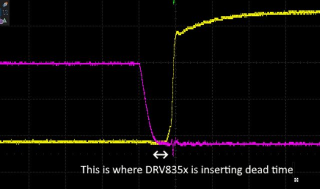
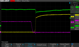
During the testing we met with the following issue, when PWM GHx goes from high to low. When INHx is pulled down, it's corresponding GHx doesn't immediately go down (see scope figure). Instead, it does so in two steps. In the first step the GHx is weakly brought down for about 400ns (not enough to switch off the MOSFET) and then after the signal is fully brought down. This only happens to GHx not GLx and causes a brief short circuit and brief error signal.

(Blue: INHx, Yellow: GHx. Purple: GLx, Green: FAULT_N, measurement was done without motor, having zero current)

We increased/decreased the IDRIVE resistor, but the curves are the same, only the rate of signal rise or fall changes.

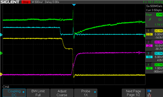
In the opposite case, when GHx goes low to high works properly as it is indicated on the figure below (the only issue is that the deadtime seems to me 500ns instead of the 100ns mentioned in the datasheet)

Could you suggest some solution to solve the issue during turn-off of the upper transistor?

Thanks in advance

  • Hello Mr. Stumpf,

    Can you share your schematic file so we can confirm the connection between the DRV835x and MOSFETs?

    Are you using the hardware interface (DRV8350RH) or the SPI interface (DRV8350RS)?

    I am noticing that nFAULT does not actually pull all the way down to 0V - so this event could either be a fault or ground bouncing.

    Dead time in the DRV835x is inserted between HS gate OFF (<2V) and LS Gate start to turn ON, or LS gate OFF (<2V) and HS gate start to turn ON. In your second image - DRV835x dead time does not include the slewing of the MOSFETs.

    Thanks,

    Matt

  • Dear Matt! Thank you for your reply. I used the RH (hardware version). I attach the schematics in the pdf. As it is a subpart of a bigger circuitry I deleted some parts (like current/voltage sensing, protection, digital interface...) and I present only the circuit components which relate to the DRV.

    Thank you in advance,

    Peter

     3833.Schematics.pdf

  • Hello Peter,

    When looking at your waveforms in the first plot, I noticed that the GLx and GHx voltages had “2X” and “0.5X” displayed on their respective ports. Just for clarification, does your first plot show that the peak of GLx is ~11V, and the peak of GHx is ~36V?

    Also, the waveform that you sent for GHx appears to be with respect to ground. It would be useful if you sent the following waveforms on the same plot:

    • GHx with respect to ground (1)
    • SHx with respect to ground (2)
    • GLx with respect to ground (3)
    • GHx with respect to SHX (1 – 2)

    Also, could you please change the timescale of these plots to be a bit smaller (100ns per division)?

    The second and last waveform I have requested will be very useful in telling us the high-side VGS after the first spike, which will allow us to infer certain things about what is occurring.


    Best,

    Johnny