This thread has been locked.

If you have a related question, please click the "Ask a related question" button in the top right corner. The newly created question will be automatically linked to this question.

DRV8302: DRV8302 X-ray inspection - faulty boards

Part Number: DRV8302

Hi, 

We just recently had a new production for our Motor controllers that are using DRV8302, this wasn't the first production and we had another production 6 months prior to the latest one and in the new production, we witnessed some new issues.

Please keep in mind that all the production line is automated and No manual or hand soldering was involved in SMD assembly of these boards.

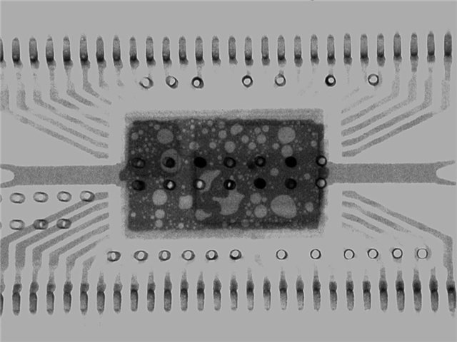
- We witnessed around 25% failure rate in the production line after testing the boards due to issues with DRV8302, so to inspect it further, as the design was tested lots of times, and we never had an issue with DRV8302, we did an X-ray inspection for 6 sample boards as their images are also attached in this post, you can find the explanation for each below:

X1: It is the working sample right after the production for your reference, so we can name it the GOLD board.

X2 and X3 : samples without switching at the output, these two boards are just programmed right after the production and they failed to produce any output at the switching stage ( nFault is Low), the Buck converter works and we see the +5V output ( as designed for)

X4, X5 and X6: These are the boards that we witnessed the Buck converter is not regulating the voltage and the input voltage is appearing directly at the output, as a result, all the components connected to  this are sparked and destroyed. ( rare condition, maybe 4% of all the failed boards)

_ Test condition: all the boards are powered up with 50V at the input ( our standard test for all the boards)

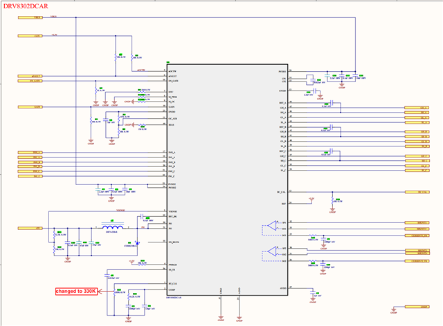
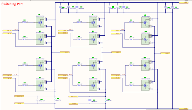
In all these Images, U1 is the DRV8302, and the Q3 to Q14 are the Mosfets connected to DRV8302 ( we used parallel MOSFETs on each side)

Based on my observation I understand the following:

for X1 ==> The soldering of the power pad is not great, but there is some sort of a return path for the ground plane ( still IMO this is not a good one), but the board works and DRV8302 doesn’t show any fault and we can see the switching at the output of the Mosfets, although I feel the Mosfets pads are not also very well connected and possibly the line impedance is not very low...

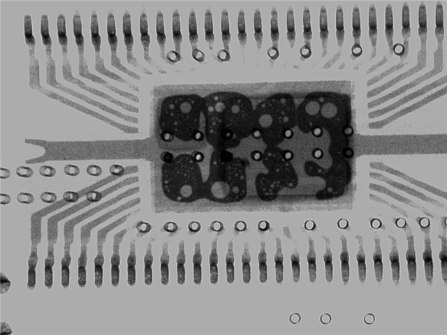
For X2⇒ the power pad connection is poor and it seems there is some sort of an island between the ground of the Buck to the other ground of the IC


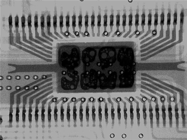
For X3 ⇒ it seems the DRV is well connected but there is some sort of an issue with the Mosfets soldering…

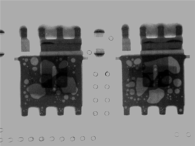
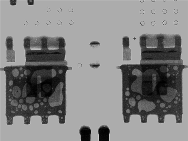
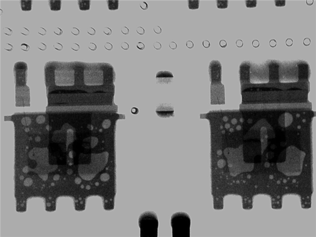
for X4, X5 ⇒ it’s evident that the Buck converter doesn’t have a good return path or it’s insulated from other paths, so it can’t close the loop...

Now we are in discussion with our manufacturer and they are not very well convinced that the issue is with solderings while we previously manufactured the same boards with another manufacturer and we didn’t have this issue.

So I’d like to know what are the thoughts of the TI design and manufacturing team on this and have you ever witnessed such issues in production lines?

Regards

John

DRV8302_Xray.zip

  • Hi John,

    Thanks for posting on the MD forum, sorry to hear you're having trouble with the device.

    With at 25% failure rate this may be an issue with your schematic/layout. Can you post your schematic so I can review it? (if needed I can review the layout too but let's start with schematic).

    Were you able to successfully spin a motor for a period of time before seeing the failure happen? 

    I see that none of this was soldered by hand, and it was all done on the production line. For the units that are failing (X2-X5) have you tried to remove the units and clean them, clean the pads, and re solder the units back on to see if this resolves the issue? What if you put a brand new DRV8302 on (by hand)?

    We need to get to the root cause of what's causing the very high failure rate. Is it schematic related or is it production line related? That's what we need to figure out.

    What changed from V1 of this board to V2? 

    Regards,

    Michael

  • Hi Michael, 

    sorry for the delay, the notification from the TI forum ended up in my spam folder, so I didn't notice that, I'll go as below:

    Were you able to successfully spin a motor for a period of time before seeing the failure happen? 

    all the boards with problems are unable to apply switching at the output to the MOSFETs, subsequently, right after start-up (power-up) there is no output from DRV8302 toward the MOSFETs, and of course, it's not possible to spin a motor.

    I see that none of this was soldered by hand, and it was all done on the production line. For the units that are failing (X2-X5) have you tried to remove the units and clean them, clean the pads, and re solder the units back on to see if this resolves the issue? What if you put a brand new DRV8302 on (by hand)?

    Yes, for some of them we changed the DRV8302, and they started to work and some didn't, also for some we applied heat over the DRV8302 and Mofet region and they started to work without changing any components, but again the root cause of the problem as you mentioned is unclear. we have lots of boards like that and we can't just test them 1 by 1 to see what happens as each one tested manually will lose its quality to be sold to the customers.

    What changed from V1 of this board to V2? 

    Nothing in the Power and switching side, as far as I remember the layout of DRV8302 and the Mosfets remained intact, we just added some new features in the Signal and low power side.

    But 1 major question, from my X-ray files, do you see any defects, or do they look normal? to me, they are not well soldered and the Power pad of DRV8302 is randomly connected to the PCB, as well as lots of holes in the Mofet pad, this is very important to clarify if TI has some standard for the production quality of their chips, also for Stencile design of the PCBs.

    Here is the Schematics for the DRV8302 and the Mosfets ( all the gate paths are done with length control, and the shunts are routed differentially)

    Regards

  • Hi John,

    I've reached out to our packaging team to review the Xrays. Once they provide feedback I'll pass it onto you, which will probably be tomorrow. I didn't have time today to do an in depth schematic review, but I'll get to it tomorrow. Thanks for your patience. 

    Regards,

    Michael 

  • Hi John,

    I'm still waiting on feedback from the packaging team. The fact that you were able to remove the DRV, re solder a new one on, and then you had success spinning a motor, leads me to believe that this is a soldering issue. You said this worked on some of the boards, but on other boards the problem still persisted (after replacing DRV). For the boards you did replace the DRV and could spin a motor, were you able to spin a motor for a significant amount of time without any failure?  

    Some thoughts on your schematic

    - Since you are powering these boards with PVDD = 50V, it's best to have your bulk capacitance at twice the rated voltage of your input voltage. So I'm recommending C24,C27, and C32 get replaced with 100V rated caps. Since this power stage worked fine on your previous version of the board, I don't think this is an issue. However if there is ever a version 3 of the board, it may be worth changing. 

    - I'm assuming this is a high current application since you're using MOSFETS in parallel. Was there any damage to the MOSFETS in these tests? I see you said the MOSFETS are still intact, I just want to verify I'm understanding that they are not damaged. 

    - As for the DRV schematic, it seems like you followed the application section from the datasheet and it looks good. 

    I've reached out to the packaging team again today to try to get you an update as soon as possible. 

    Regards,

    Michael

  • Thank you, Micheal, 

    Since you are powering these boards with PVDD = 50V, it's best to have your bulk capacitance at twice the rated voltage of your input voltage. So I'm recommending C24,C27, and C32 get replaced with 100V rated caps. Since this power stage worked fine on your previous version of the board, I don't think this is an issue. However if there is ever a version 3 of the board, it may be worth changing. 

    Thanks for the suggestion, but in faulty boards, we see the error regardless of the Bus voltage value, for instance at 24V or even lower than that, so I believe this might not be an issue, but yes, in the next iterations, we will consider increasing the voltage rating of those caps ( if the form factor allows us).

    For the boards you did replace the DRV and could spin a motor, were you able to spin a motor for a significant amount of time without any failure?  

    Yes, it seems there were no other issues as soon as they started to work and they behaved like a normal board in all the conditions

    - I'm assuming this is a high current application since you're using MOSFETS in parallel. Was there any damage to the MOSFETS in these tests? I see you said the MOSFETS are still intact, I just want to verify I'm understanding that they are not damaged. 

    as far as I see, there is no diagnosable damage to the MOSFETs, both visually and operationally, meaning that the MOSFETs are not causing any short or overheating or excessive current drain, so I can imagine they are fine.

    I should say that since right after the Power up the DRV goes into fault mode, the MOSFETs are not switched at all, so there is a very little chance that they get damaged in this condition, as also there is no load connected to the board and there is no stress on the MOSFETs in initial tests.

    I've reached out to the packaging team again today to try to get you an update as soon as possible. 

    ok that will be great, also I appreciate it if they can offer the best Stencil pattern design for both the DRV power-pad and SMD MOSFETs, as you see the Stencile designed by our manufacturer are like those little squares that are segmented, and during heating, they become like islands and not molten well, and I'm not even sure that's the right way to do this.

    BTW, I'll be waiting for your packaging team analysis, and let's see what they say.

    Regards

  • Sounds good John,

    I'll update you as soon as I have feedback.

    Thanks,

    Michael

  • Hey John,

    The packaging team got back to me with some feedback on the X-Rays you provided.

    The DRV8302 is a HTSSOP Power-Pad device.

    The datasheet includes a package drawing with PCB pad and stencil recommendation. Based on the images above, it seems that your stencil has 8 smaller opening instead of one opening. The datasheet suggest a stencil opening of 6.35 X 3.61mm with 0.127 thick stencil. Those holes are thermal vias, we suggest to plug or filled these to avoid solder wicking into the vias. During SMT, the package should release after touching the PCB, not release at the point when just touching the solder paste or free fall above the solder paste.

    I have attached an App Note for this type of package for reference. Here's the link

    I hope this helps, let me know if you have any further questions.

    Regards,

    Michael

  • Thank you, Michael, I will share this valued information with our manufacturer and I will ask them for modification of the stencile's apertures as it's not matching with the suggested pattern ( the aperture in the Gerber files delivered is exactly like the datasheet, but IDK due to what strange reason they decided to make it with 8 separate openings !!! )

    the last question:

    During SMT, the package should release after touching the PCB, not release at the point when just touching the solder paste or free fall above the solder paste.

    I can imagine this should have some standard, I mean for SMT machine programming, is there any value for setting the force of pressure for the placement of component to the PCB for DRV8302 on top of the solder paste? 

    I'm asking all these questions to avoid any problem with our next production, as it's very critical for us to reduce the number of controllable errors to zero.

    Thanks in advance for your great support.

    John

  • Hey John, 

    I will reach out to packaging for more advice on a standard for SMT machine programming. It's a good question, how much force/pressure to apply to the DRV so it makes good electrical contact with the solder and thus the pads. 

    Thanks,

    Michael

  • Hi Michael,

    It turns out we have some news from the manufacturer and this is what they say:

    "Inside our company, Gerber files received from any client are always checked and processed in order to achieve the best results.

    Choices are made based on our equipment capabilities, IPC regulations, and all the experience our team can put into any project.

    We know the *recommended patterns shown in datasheet files, but we also know real world isn’t always as described on paper.

    Truth is almost all solder joints shown on X-rays fall inside IPC acceptability-rate. Very few would be marked as not acceptable, needing rework.


    Focusing on boards not working -

    During last week we tried substituting component U1 on faulty boards (marked as “NO Output”).

    After replacement of driver component U1, the requested square wave appeared on the output.

    It is important to note we did not make any other change other than replacing component U1:

    no heat whatsoever on other regions of the board, and no mechanical push of components.

    To confirm this result, we reassembled back “faulty U1” on working boards, confirming U1 was not working properly.


    I might be wrong, but to me these latest clues seem to suggest a faulty batch of components U1.

    We would like to go on substituting U1 on all faulty boards, in order to confirm the fix.

    Please note: latest batch of 20 components “U1” were bought from different supplier, with cost 3 times higher than previous production batch.

    We’re collecting all faulty components for further investigation, if needed."

    So they believe those PowerPad solderings falls into their "IPC standards" and the problem is with a broken batch of DRV8302, which to me can not be the definitive reasoning, as bad soldering can cause damage to DRV right after power up and it's not possible to say the DRV was broken from the begining.

    I know it's a complicated situation, but I believe it can be interesting for the DRV team to see high-volume production issues that might arise using these cool chips ( I'm a hardcore TI fan, love the way you guys work ).

    anyways, what are your thoughts on this too?

    Regards
    John

  • Hi John,

    Please note: latest batch of 20 components “U1” were bought from different supplier, with cost 3 times higher than previous production batch.

    Can you send me some pictures of the IC's themselves? It's possible that they are counterfeit devices if they were not purchased from TI or one of our providers. I'd like to see pictures of both the failed units and the units that are working. We can verify if these are counterfeit parts or not. As for if there was a bad 'batch' of these devices, I don't know. I'll have to check internally. 

    We would like to go on substituting U1 on all faulty boards, in order to confirm the fix.

    Yes please try that and let me know results. 

    I know it's a complicated situation, but I believe it can be interesting for the DRV team to see high-volume production issues that might arise using these cool chips ( I'm a hardcore TI fan, love the way you guys work ).

    It is very strange, but we shall figure this out. Thanks for the support John,  we're always happy to help. 

    It seems that the manufacture for your boards is very confident that it's not a soldering related issue.

    Feedback from the packaging team

    "For packages with leads like SO, TSSOP, QFP etc. Most of the stress after mounting on PCB is at the heel.

    So the best way to form a good solder fillet at the heel that provides good reliability is to set the package to sit on the PCB pad so that solder paste is wrapping around the lead. For leadless package like QFN and SON. We want the package to settle in the middle of the solder paste so that it doesn’t apply too much pressure and squeeze the solder paste out."


    Regards,

    Michael

  • Good Morning John,

    Would it be possible for you to provide us with the stencil files so we can review them? If so please include the stencil thickness.

    In addition, try to find out how the package was mounted onto the PCB. 

    Regards,

    Michael

  • Hi Michael, 

    Sure, I'm in contact with them and hopefully they provide me the Images to check the counterfeit scenario plus the stencil files, but let's see, we are approaching the holiday season and things are not predictable now.


    I will get back to you immediately after I have some info from their side.

    Thanks
    John

  • Hi Michael, I've just sent you the pictures of good and faulty DRVs plus the Stencil files used in our production in PM, so pls have a look and let us know your thoughts
    Regards
    John 

  • Hi John,

    Sounds good, I'll take a look.

    I'm going to close this thread, we can finish the rest of this over PM. 

    Thanks,

    Michael