This thread has been locked.

If you have a related question, please click the "Ask a related question" button in the top right corner. The newly created question will be automatically linked to this question.

DRV8601ZQVEVM: DRV8601 driving a LRA

Part Number: DRV8601ZQVEVM

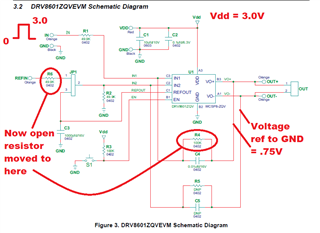
DRV8601ZQVEVM development board.
When I connect VDD = 3.0V I expected to see VDD/2 on VO+ and VO-. Instead of seeing 1.5V referenced to GND on each pin, I see 1/2 that amount. I see .75V Why?
I see the same voltage on REFOUT
JP1 is in the 2-3 position. No PWM is connected, only VDD.
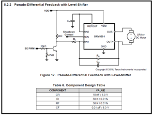
When I do connect a PWM, VO+ and VO- offset remains the same.
The LRA runs but I do not see the P-P that I should. I changed R4 to a 49.9K to negate the gain of 4.
In this configuration I make sure the PWM signal high level = VDD.
I am trying to duplicate the circuit shown on page 11 of the datasheet.
Why am I not seeing VDD/2?

  • Hey Mike,

    So have you tested the pin voltage with JP! in 1-2 configuration?, and is there no R2 and R5 as well in the schematic since you are replicating that set-up on p.11?

    A picture of the circuit would be helpful in trying to find the problem.

    Best,

    Carson 

    Low Power Audio

  • My guess is I am overlooking something very simple.

    Here is the modification to the development board. Vdd is 3.0V regulated.

    I expected 1.5V instead of .75V on each line to the LRA. What am I missing?

    Here is the circuit we believe is correct for our application and it gives us the most flexibility for any LRA we wish to use.

    We will be using an adjustable LDO for Vdd

    I did not incorporate the mosfet in the Dev board. I just insure the logic level on the PWM = Vdd for testing purposes.

    Thanks

  • Hey again,

    So can you clarify if R2 or R5 are on your board or not?

    Regards,

    Carson

  • R2 is present and both R5 and C5 are not populated.

    Those areas were unmodified. They are as documented.

    The only change we made was replaced R4 with resistor taken from R6. R6 remains unpopulated.

  • Hey Mike,

    R2 should not be there according to schematic you are trying to follow. Please remove and let me know if the issue persists.

    Best,

    Carson

  • Let me guess, The output impedance of REF out is high so the R2 to GND creates a voltage divider. Poor assumption on my part thinking that 49.9K would not be an issue. I checked the datasheet  to see if there is any reference to output impedance on REFOUT and I did not see any. Maybe for a future update or a mention in the DEV board doc? I will have the board modified and report back. Stay tuned.

  • Mystery solved. Since the resistor is only shown on the development board it would be helpful if something was mentioned about R2 and why it should be removed. Thanks for all the help!