Hello, dear experts:
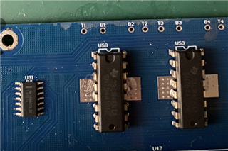
We have used SN754410 and maintained the same circuit design for many years, but occasionally the chip conversion failure occurred.
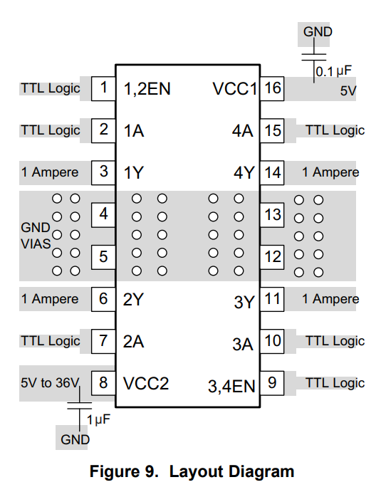
We use SN754410 to convert 3.3V-LVCMOS level input pulses into 15V level PWM signals and send them to the IGBT driver card.
The input signal adopts a 3.3V open-drain circuit with a 510Ω pull-up resistor, please refer to the following circuit:
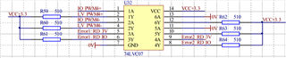
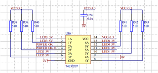
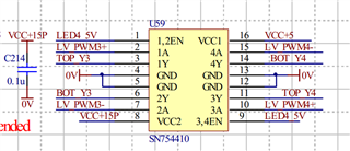
LED4_5V is actually 3.3V, and the pull-up resistor is also 510Ω.
The PWM signal in our product occasionally fails. After no-load test, it is found that the output signal of 1 of the 4 outputs is often low, but the corresponding input signal still has the expected LVCMOS level pulse (2.5KHz, 50% Duty). ). After a period of time, this Pin can resume normal 15V pulse output.
The pin with the output problem is not fixed yet, sometimes it is 2A, sometimes it is 3A.
LED4_5V is actually 3.3V, and the pull-up resistor is also 510Ω.
The PWM signal in our product occasionally fails. After no-load test, it is found that the output signal of 1 of the 4 outputs is often low, but the corresponding input signal still has the expected LVCMOS level pulse (2.5KHz, 50% Duty). ). After a period of time, the Y can resume normal 15V pulse output.
The pin with the output problem is not fixed yet, sometimes it is 2A, sometimes it is 3A.
I would like to know, under what circumstances will SN754410 fail to convert, I am not sure if this performance of the chip means that it has been damaged.
My English is not very good, thanks for the help