This thread has been locked.

If you have a related question, please click the "Ask a related question" button in the top right corner. The newly created question will be automatically linked to this question.

[FAQ] DRV8353: Protection trigger and GUDV abnormality of DRV8353 at high current

Part Number: DRV8353

Hello, I am a TI FAE, we want to know if the MOSFET and half bridge circuit may cause permanent damage to the internal drive circuit and charge pump of DRV8353 when DRV8353 works at high current. If so, what is the damage mechanism?


Here are the details:


This problem is based on links

e2e.ti.com/.../3694693 tisearch=e2e-sitesearch&keymatch=DRV8353#3694693


In the last consultation, we did not solve the problem of two-phase protection of the system under high current.


However, at present, we are temporarily focusing on solving the problem of DRV8353 triggering protection when working with high current. The main purpose of this post is to know the specific triggering reason of protection.


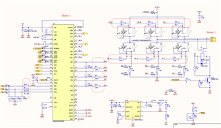
The circuit diagram is shown below. Now we pay more attention to the threat to the charge pump and drive circuit of DRV8353 when the half bridge composed of MOSFET flows through high current.


At present, we have made the following attempts:


When we keep the detection and protcetion about GH_ A/GL_A and SPN/SNA , the current increases due to artificial loading on the motor. When the motor current reaches 60-70A, DRV8353 triggers some protection, but SPI cannot work at this time, so it is impossible to know what protection is triggered.


However, in my opinion, this does not trigger the overcurrent protection, because the OCP is set at 200A in this case, and the DRV8353 does not trigger the protection immediately when the current reaches 60-70A, but only after a few seconds. So we began to explore what kind of protection DRV8353 triggered.


So we close GH_ A/GL_ A and SPA/SNA detect and protect the motor at the same time. The first problem is that the over temperature protection is triggered. It should be noted that the over temperature object here is not DRV8353, but MOS tube. This is caused by the temperature rise of MOS tube. MCU detects that the temperature of MOS tube is too high, so it turns off DRV8353.


We turned off the over-temperature protection and continued the same experiment. Under similar working conditions, the power supply triggered the over-current protection. However, this power supply will trigger protection only when there is serious overcurrent, which indicates that there may be a problem that makes the instantaneous value of current very large.


However, different from the previous situation, when we restart the system, we find that GDUV fault occurs, which is known by checking the register of DRV8353. No matter how to restart or reset, this problem cannot be eliminated. We believe that in the last experiment, some processes of the power circuit led to the permanent damage of the charge pump or drive circuit in the DRV8353.


It should be noted that all the above experiments are not triggered immediately when the current reaches 60-70A, but after repeated locked rotor for several times, which is a process that needs to be accumulated. In other advisory posts on DRV8353, GDUV abnormalities also occur to many engineers under high current or high Vdrain, so I think this is a common application problem.


I also hope you can try to give some possible wrong directions and solutions, thank you!

  • Hi Dong,

    I am going to break this reply down into multiple sections. 

    Overcurrent Protection (OCP)

    VDS overcurrent protection is simply monitoring the VDS voltage for the HS MOSFET (VDRAIN to SHx) and LS MOSFET (SHx to SPx) and ensuring that the measured VDS voltage exceeds the VDS_OCP value for longer than the overcurrent deglitch time (tOCP_DEG). This is the recommended overcurrent protection method to use with the DRV8353. 

    Overcurrent protection can also be sensed through the shunt resistor (SEN_OCP). VSEN overcurrent protection is simply monitoring the differential shunt voltage (SPx-SNx) and ensuring that the measured shunt voltage exceeds the VSEN_OCP value for longer than the overcurrent deglitch time (tOCP_DEG). This is the recommended overcurrent protection method to use with the DRV8353.

    SPI

    You say SPI cannot work when current reaches 60-70A, may you explain further what you mean? Do you lose communication with the DRV8353? Do registers get reset or do frame errors occur? This should not occur. 

    Gate drive related

    Gate drive faults occur if the gate is not in its expected state (ON/OFF) after the tDRIVE period. A gate is considered "ON" if VGS > 2V, and "OFF" is VGS < 2V. Gate drive waveforms are determined by the gate current turning on/off the MOSFET, and there should be a distinct "Miller" plateau when turning on/off the MOSFETs - this is when the MOSFET VDS rate slews. It is also good to note that we should try not to slew VDS too fast (i.e. 100ns or less), or else we run the risk of slamming on/off the MOSFETs too fast and causing very noticeable SHx overshoot/undershoot. Another consequence is that if there is parasitic inductance on the board layout, it is possible that voltage spiking can occur and couple into the LS MOSFET's gate, causing potential shoot-through.

    The main takeaway from all this is that gate drive current is the critical factor in ensuring the MOSFETs turn on or off correctly to not induce a gate drive fault but to also slew the VDS voltage of the FETs at a slew rate that can commutate the BLDC motor without risking any damage to the FETs or DRV device. 

    Schematic related

    Since there is a large amount of current and this is a high power motor application, there are many things with the schematic I would like to provide feedback:

    - What is the IDRIVE setting used for this application? Since the FETs have a Qgd = 16nC, we recommend IDRIVE ~ 80mA for a VDS rise/fall time of 200ns 

    - Any reason for having 0 ohm resistors for GHx and 2.2 ohm resistors for GLx? GLx having 2.2ohm resistors shouldn't hurt the gate drive current, but evaluation with appropriate IDRIVE settings is recommended first. Use only series gate resistors if a setting lower than the smallest IDRIVE setting is needed or a gate drive current between settings is required

    - For higher power BLDC motor designs, we highly recommend this app note: System Design Considerations for High-Power Motor Driver Applications

    - We recommend the following components for "tuning" the power stage in the case of transients going back to the supply, FETs, and/or gate driver:

    - >1uF capacitor(s) from VDRAIN-GND (close to HS FET's drain) to remove positive transients from bus voltage sourcing into the switch node when the HS FET is turned on. 

    - 0.1-1uF capacitor from VDRAIN-SPx to remove negative transients from SPx and not violate abs min spec

    - RC snubbers for each FET if oscillation occurs when switching on/off SHx, this removes switch node ringing and improves EMI and/or potential noise coupled into the low side gate

    - I notice a split ground (PGND/DGND/AGND). How are these grounds connected? Ensure there is low inductance between these connections, we want to ensure that there isn't any PGND potential or noise or else this can cause VSEN_OCP protections to trigger if the GND is higher than 0-V. 

    Measurements (if possible)

    - Since VSENSE protection is used, has the SPx-SNx voltage been measured?

    - Since it is unknown which phase(s) the overcurrent faults or gate drive faults occur, has there been any measurements taken on a phase's INHx, GHx, GLx, and SHxt? Want to ensure the waveforms are turning on correctly and see if overcurrent has been triggered by nFAULT going low. 

    Layout

    It may be good to inspect the layout is as well, we can review this as need. Would the customer be willing to send the layout?


    Thanks,

    Aaron

  • Hi Barrera,

    I will confirm the information with the engineer as soon as possible, and then reply to you in time. This project is very important to me. Thank you for your support!

    Thanks,

    Sanders Shen

  • Hi Dong,

    Sure thing, please keep me updated and I will be happy to support! Note I will be out of office the next two business days, and next Monday is a holiday in the U.S. so a teammate can will support you until I return. 

    Thanks,
    Aaron

  • After consulting the questions of others in E2E, I found that this is a common problem. After communicating with colleagues who have experience in high current project, he also pointed out some possible solutions to me.

    In the near future, I will learn the professional knowledge of gate driver and MOSFET on and off, and also read the user manual on high-power motor drive provided by BU.

    After I have made further progress, I will continue to reply in this post. Thank you!

    Sanders Shen

  • Thanks Sanders!

    Please do let us know when you have additional questions

    Thanks,

    Matt

  • Hello Sanders,

    May I close this thread? You can always click the "Ask a related question" button.

    Thanks,

    Matt

  • Hi Sanders,

    I'm going to go ahead and close this thread. If you have further questions, please click the "Ask a related question" button.

    Thanks,

    Matt