


Two questions:
1. Buck output problem
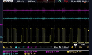
DRV8350RS has a 12V to 3.3V step-down,
The PWM waveform of the SW output point sometimes appears as shown in the figure below, which is not a stable PWM output waveform.
What are the reasons for this situation? And is there any way to solve it?
Purple: FB point feedback voltage
Blue: SW point output PWM voltage after inductance
Yellow: SW point output PWM
2. About GND point configuration
In the datasheet, we did not find any suggestions on the GND point configuration.
Should the GND point be close to the high voltage or the GND terminal of the signal?
What is the impact of the difference between the two placements on the DRV8350R?
And what is the recommended configuration location?


